* On your first PCB Assembly order!
* Up to $300 discount
 C - A L L E Y
 Home | Events | PCB | About Us | News | Contact Us
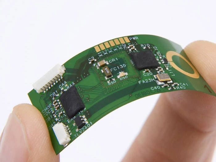
Design for Manufacturability (DFM) is essential in PCBA development to ensure products are efficient to produce, cost-effective, and reliable. Below are key DFM considerations for optimizing PCBA design.
1. PCB Layout Design
A well-planned layout improves both manufacturing efficiency and product performance. Begin by grouping components functionally and positioning frequently accessed or fragile parts in accessible locations. Maintain adequate spacing between components to facilitate soldering, inspection, and rework, while avoiding unnecessary gaps that increase board size. Additionally, reserve appropriate space for larger components such as heat sinks and connectors.
2. Pad Design
Pads must match component lead specifications in size, shape, and spacing. Oversized pads can cause solder bridging, while undersized pads may lead to weak joints. Select pad shapes—such as round, rectangular, or oval—based on the component type. Ensure pad spacing complies with soldering process capabilities to prevent shorts or open solder connections.
3. Routing Design
Keep traces short and direct, minimizing vias and avoiding unnecessary bends. For high-speed signals, carefully manage impedance and signal integrity to reduce delay and distortion. Choose trace widths according to current requirements to ensure sufficient current-carrying capacity and prevent overheating.
4. Test Point Design
Incorporate accessible and logically distributed test points to support in-circuit testing (ICT) and functional validation. Ensure test points are placed away from tall components and allow clear probe access. Cover all critical nodes to improve fault detection and troubleshooting efficiency.
5. Material Selection
Select PCB materials and components with manufacturability and reliability in mind. Choose substrate materials based on operational environment, thermal needs, and signal performance. Source components from reputable suppliers with stable availability, and consider package styles and pin pitches that are compatible with automated assembly processes.
Conclusion
Integrating DFM principles early in the design phase significantly reduces production issues, accelerates time-to-market, and enhances product quality. At KingshengPCBA, we provide professional DFM analysis and support to help optimize your designs for seamless manufacturing.
Reach out to us to ensure your next PCBA project is both high-performance and production-ready.

Please send Email to kspcba@c-alley.com or call us through +86 13828766801 Or submit your inquiry by online form. Please fill out below form and attach your manufacturing files( PCB Gerber files and BOM List) if need quotation. We will contact you shortly.
 +86 13828766801
 kspcba@c-alley.com
 https://www.kingshengpcba.com/
 2/F, Building 6, Tangtou 3rd Industrial Zone, Tangtou Community, Shiyan Town, Baoan District, Shenzhen, China, 518108
We would also like to thank our customers for their trust and support. The company's outstanding achievements are mainly due to the loyalty of our customers, which also encourages and spurs our company to forge ahead.


