* On your first PCB Assembly order!
* Up to $300 discount
 C - A L L E Y
 Home | Events | PCB | About Us | News | Contact Us
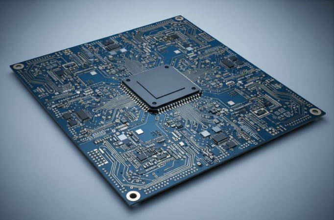
Within the electronics manufacturing sector, Printed Circuit Board Assembly (PCBA) is the core process where electronic components are assembled onto PCBs to create functional modules. The following outlines the standard workflow.
1. Production Preparation: Documentation & Material Verification
This initial phase lays the groundwork for all subsequent steps. The primary task is the preparation of all technical documentation, including schematics, PCB layout files, the Bill of Materials (BOM), component coordinate files, Gerber files, assembly instructions, and test plans. These documents provide the precise guidelines for production.
Concurrent material verification is critical. All components and materials must be rigorously checked against the BOM for specifications, quantities, and quality to ensure full compliance with design requirements, safeguarding the integrity of the entire manufacturing process.
2. SMT (Surface Mount Technology) Assembly Process
SMT is a central process in modern PCBA manufacturing for mounting components onto the board surface.
Solder Paste Printing: Automated printers apply solder paste onto the PCB pads.
Solder Paste Inspection (SPI): This step checks for printing defects like insufficient paste, bridging, or misalignment.
Component Placement: Pick-and-place machines accurately position components onto their designated locations on the PCB.
Reflow Soldering: The board passes through a reflow oven. Controlled heating melts the solder paste, forming permanent solder joints upon cooling.
3. DIP (Dual In-line Package) Insertion Process
This process is used for through-hole components.
Automated/Manual Insertion: An Automated Insertion (AI) line can be used for standard components, while specialized parts often require manual insertion.
Insertion Sequence: Components are typically inserted in order of height (shorter first, then taller). Correct orientation for polarized components is essential.
Dimensional Control: Insertion accuracy is controlled within ±0.1mm, followed by manual visual inspection.
4. Wave Soldering
Following DIP insertion, wave soldering is typically employed to solder the through-hole components.
Fixture Loading: The PCB is secured in a fixture to prevent thermal deformation.
Flux Spraying: Flux is applied to remove oxidation and promote solderability.
Preheating: The board is preheated to a temperature between 110°C and - 150°C.
Soldering: The board passes over a solder wave, which creates the solder joints for the inserted components.
Cooling: The assembly is cooled rapidly to solidify the solder joints. Parameters like preheat temperature, conveyor speed, and solder temperature must be strictly controlled to prevent defects.
5. Testing & Inspection
This final phase ensures the quality and functionality of the assembled PCBA.
AOI (Automated Optical Inspection): High-definition cameras check soldering quality. Suspect units may undergo offline re-inspection.
Electrical Testing: Tests such as In-Circuit Test (ICT) and Functional Circuit Test (FCT) are performed to verify electrical performance and full functionality against specifications.
At KingshengPCBA, we meticulously execute each of these processes, leveraging state-of-the-art equipment and stringent quality control to deliver reliable, high-performance circuit boards. Ready to bring your electronic designs to life? Contact KingshengPCBA today for a seamless manufacturing experience and expert support from prototype to mass production.

Please send Email to kspcba@c-alley.com or call us through +86 13828766801 Or submit your inquiry by online form. Please fill out below form and attach your manufacturing files( PCB Gerber files and BOM List) if need quotation. We will contact you shortly.
 +86 13828766801
 kspcba@c-alley.com
 https://www.kingshengpcba.com/
 2/F, Building 6, Tangtou 3rd Industrial Zone, Tangtou Community, Shiyan Town, Baoan District, Shenzhen, China, 518108
We would also like to thank our customers for their trust and support. The company's outstanding achievements are mainly due to the loyalty of our customers, which also encourages and spurs our company to forge ahead.


