* On your first PCB Assembly order!
* Up to $300 discount
 C - A L L E Y
 Home | Events | PCB | About Us | News | Contact Us
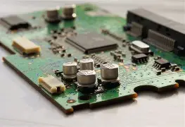
Ensuring Flatness and Reliability in High-Density Electronics Manufacturing
PCBA warpage, or board bending and distortion during production, is one of the most common and costly issues in electronics manufacturing.
Even a slight deformation can lead to solder defects, BGA cracking, poor component alignment, and long-term reliability failures.
As components become smaller and boards more complex, ensuring flatness throughout the SMT process has become critical. In this article, we explain why PCBA warpage happens and how to prevent it effectively.
Why PCBA Warpage Happens
PCBA warpage is primarily caused by thermal stress, material imbalance, and mechanical strain during manufacturing.
Common reasons include:
| Cause | Description |
|---|---|
| Uneven copper distribution | Different heat absorption/expansion across PCB |
| Improper layer stack-up | Asymmetric laminate structure causes bow/twist |
| High reflow temperature stress | Boards deform when heated above Tg |
| Moisture absorption | Humidity inside the substrate expands during reflow |
| Component thermal mismatch | CTE difference between components and PCB |
| Insufficient panel support | Flexing during reflow or handling |
Understanding these reasons helps us select targeted solutions.
Best Practices to Prevent PCBA Warpage
1. Use Balanced PCB Stack-Up Designs
A symmetrical stack-up distributes stress evenly.
Recommended practices:
-Maintain copper balance across layers
-Avoid uneven resin or copper thickness
-Choose high-Tg (+170°C) materials for high-temperature applications
Tip: HDI and multilayer PCB designers should aim for structural symmetry.
2. Control Reflow Profile & Temperature Gradients
Warpage often occurs during reflow when the temperature rises rapidly.
How to control:
-Use gradual heating & cooling (3°C–5°C/sec ramp rate)
-Maintain a nitrogen environment for temperature stability
-Apply proper soak time to reduce thermal shock
Result: Lower internal stress and improved solder reliability.
3. Moisture Bake Before Assembly
Moisture causes substrate swelling during reflow.
Recommended baking:
-120°C for 4–8 hours, depending on board thickness & storage time
-Store PCBs in dry cabinets or vacuum packaging
4. Add Mechanical Support During Reflow
Use reflow carriers, pallets, or tooling fixtures to keep boards flat.
Best for:
-Thin PCBs (<1.0mm)
-Flexible-rigid boards
-Heavy BGA or connector areas
5. Optimize Panel Design
Panelization affects board expansion and bow.
-Routing & V-cut design should avoid stress concentration
-Consider break-off points reinforcement
-Use support rails for high-density boards
6. Choose Correct Materials
Material stability matters.
| Material Factor | Recommended |
|---|---|
| High-Tg laminate | >170°C |
| Low CTE substrate | Better heat stability |
| Reinforced glass weave | Higher-dimensional stability |
Consistent materials help avoid thermomechanical distortion.
7. Avoid Manual Handling Stress
Physical bending can worsen warpage.
-Use automatic handling equipment
-Avoid manual bending during depaneling
-Use milling instead of V-cut for fragile boards
How KingshengPCBA Ensures Flat & Reliable PCBA
At KingshengPCBA, we follow strict flatness-control procedures:
-DFM review & balanced PCB stack-up suggestions
-Moisture control & prebake process
-Controlled nitrogen reflow profiles
-Dedicated reflow support fixtures
-Full AOI + X-Ray inspection for solder integrity
Our goal: Zero-warpage, high-reliability PCBA for global customers.
Conclusion
Preventing PCBA warpage requires material selection, thermal control, and engineering discipline.
With proper design and process optimization, manufacturers can ensure flatness, boost SMT yield, and improve long-term stability.

Please send Email to kspcba@c-alley.com or call us through +86 13828766801 Or submit your inquiry by online form. Please fill out below form and attach your manufacturing files( PCB Gerber files and BOM List) if need quotation. We will contact you shortly.
 +86 13828766801
 kspcba@c-alley.com
 https://www.kingshengpcba.com/
 2/F, Building 6, Tangtou 3rd Industrial Zone, Tangtou Community, Shiyan Town, Baoan District, Shenzhen, China, 518108
We would also like to thank our customers for their trust and support. The company's outstanding achievements are mainly due to the loyalty of our customers, which also encourages and spurs our company to forge ahead.


