* On your first PCB Assembly order!
* Up to $300 discount
 C - A L L E Y
 Home | Events | PCB | About Us | News | Contact Us
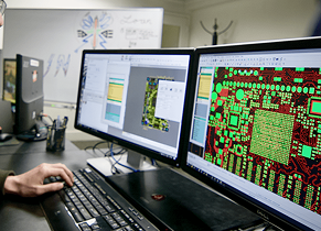
Understanding How Microscopic Structures Shape Real-World Performance
In the microscopic world of PCB design, vias act like vertical channels connecting different circuit layers — the highways for electrical signals traveling between layers.
Through holes, blind vias, and buried vias may appear tiny, but they play a critical role during SMT (Surface Mount Technology) assembly. The way a via is treated can directly determine solder joint quality, heat dissipation, and final product reliability.
1. Common Via Processing Methods, Each with Its Strengths
1.1 Via Tenting (Open via) – Heat Dissipation vs. Risk
Feature: The via is exposed with no solder mask coverage.
Advantage: Excellent heat dissipation; can serve as a test point.
SMT Concern: Solder may flow into the via, causing insufficient solder volume, voids, or bridging short circuits.
1.2 Via Covering (Tented via) – Basic Protection
Feature: Solder mask ink covers the via pad; a small amount may flow into the hole.
Advantage: Prevents solder loss during reflow; suitable for standard designs.
SMT Concern: Uneven via surfaces may cause poor wetting, solder beads, or incomplete joints.
1.3 Via Plugging (Filled via with ink or resin) – For High-Density Designs
Feature: Via hole filled with non-conductive ink or resin, then covered by solder mask.
Advantage: Prevents solder wicking and short circuits; ideal for HDI (High-Density Interconnect) boards.
SMT Concern: The process is complex and requires strict control of fill uniformity and curing quality.
1.4 Resin-Filled Via – The Best Choice for “Via-in-Pad” Designs
Feature: The hole is filled with resin, polished, and plated flat (0.15–0.55 mm diameter).>
Advantage: Creates a perfectly sealed and flat surface, safe for use under BGA (Ball Grid Array) pads; greatly improves solder joint yield.>
SMT Concern: High process precision required; resin quality directly affects reliability.
1.5 Copper-Filled Via – For High-Current Applications
Feature: The hole is filled with conductive copper paste, then plated flat (0.15–0.55 mm diameter).
Advantage: Dramatically increases current-carrying capacity and conductivity while blocking solder flow.
SMT Concern: Complex and costly; suitable for power electronics and high-reliability applications.
2. Via Design Rules, Details Define Success
When laying out vias, designers should follow these key guidelines:
1. Minimum Hole Size
2. Through-hole diameter ≥ 0.2 mm (8 mil)
Blind/buried via diameter ≥ 0.1 mm (4 mil)
3. Avoid Pads on Micro Components
4. Never place vias directly on 0402 or smaller pads, or solder paste may drain away, causing opens or insufficient solder
5. Maintain Safe Spacing
6. Via-to-via distance ≥ 0.5 mm to prevent barrel cracking or annular ring damage
7. BGA Area Restrictions
8.Never use exposed or tented vias beneath BGA solder balls
Resin-filled or copper-filled vias are the only safe options for via-in-pad applications
3. Choosing the Right Via Strategy for SMT Orders
To simplify this complex process, Linzhuo PCBA’s DFM (Design for Manufacturability) analysis helps engineers identify potential via-related risks before production.
Automated Via Rule Checking
Detects undersized vias (<0.2 mm), insufficient spacing (<0.5 mm), and exposed vias under BGAs.
Flags vias placed on fine-pitch pads (0402 or smaller) and checks mask definitions for correct processing (open, covered, or filled).
Smart Process Recommendation
When design files are uploaded, the system automatically recognizes via types and recommends the most cost-effective process — resin-filled or ink-filled vias — to match factory capabilities and avoid quoting errors.
Risk Pre-Warning and Optimization
Before order submission, the DFM tool highlights potential manufacturability issues and provides actionable modification suggestions, saving time and communication during engineering review.
With verified via design and optimized process selection, manufacturers can achieve consistent quality, shorter lead times, and transparent costs from PCB fabrication through SMT assembly.
Vias may be microscopic, but they're vital to the performance and reliability of every PCB.
Their design and processing represent the delicate balance between electrical performance, thermal management, and cost efficiency.
At KingshengPCBA, we specialize in one-stop PCB and PCBA manufacturing, combining engineering expertise with advanced DFM tools to help clients optimize via design, improve SMT yield, and achieve higher reliability.

Please send Email to kspcba@c-alley.com or call us through +86 13828766801 Or submit your inquiry by online form. Please fill out below form and attach your manufacturing files( PCB Gerber files and BOM List) if need quotation. We will contact you shortly.
 +86 13828766801
 kspcba@c-alley.com
 https://www.kingshengpcba.com/
 2/F, Building 6, Tangtou 3rd Industrial Zone, Tangtou Community, Shiyan Town, Baoan District, Shenzhen, China, 518108
We would also like to thank our customers for their trust and support. The company's outstanding achievements are mainly due to the loyalty of our customers, which also encourages and spurs our company to forge ahead.


