* On your first PCB Assembly order!
* Up to $300 discount
 C - A L L E Y
 Home | Events | PCB | About Us | News | Contact Us
Insights from a One-Stop PCBA Manufacturer
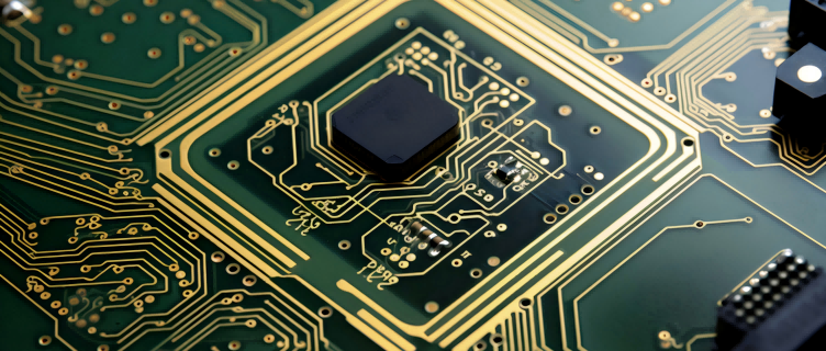
In high-end electronic manufacturing, multilayer PCBs with 8 layers or more have become the mainstream choice for complex circuits and compact designs. However, based on our years of production experience, we’ve observed that warpage during PCBA processing is significantly more common in high-layer boards. This article explores the root causes and provides proven strategies—drawn from real cases on our SMT production line—to help you minimize PCB deformation and improve assembly yield.
1. Material Factors Leading to Base Deformation
CTE Mismatch Between Materials: A multilayer PCB is composed of stacked layers of FR-4 substrate, copper foil, and prepregs. The coefficient of thermal expansion (CTE) among these materials can differ by 3–5 ppm/°C. When the layer count exceeds ten, cumulative expansion differences along the Z-axis increase dramatically, creating internal mechanical stress.
Uneven Copper Distribution: Data from production tests show that when the copper area difference between the two sides of a PCB exceeds 40%, warpage after reflow soldering can increase by up to 2.8 times. In HDI boards with blind and buried vias, this imbalance is even more pronounced, leading to local deformation during heating and cooling cycles.
2. Structural Design and Internal Stress Imbalance
Lack of Layer Symmetry: Our production analysis found that non-symmetric stack-ups in 12-layer PCBs increase the risk of warpage by over 60%. We recommend using balanced stack-up designs, such as “3+6+3” or “4+4+4” configurations, which can reduce deformation by approximately 40%.
Improper Via Distribution: Dense via arrays—especially microvias smaller than 0.2 mm—can cause localized stress concentration. For BGA areas, we suggest using staggered via layouts and ensuring a minimum copper wall thickness of 25 µm to enhance structural stability.
3. Key Process Factors in Manufacturing
Lamination Process Control: During multilayer lamination, we apply a gradual heating curve (3–5°C per minute) combined with step pressure control (30–50 psi). Compared with conventional lamination, this process reduces interlayer residual stress by up to 38%.
Surface Finish Selection: Experiments show that ENIG (Electroless Nickel Immersion Gold) surface finishes reduce warpage by 0.12 mm compared to OSP coatings on 12-layer boards. For high-layer PCBs, ENIG or immersion silver finishes are strongly recommended for better flatness and oxidation resistance.
4. Accumulated Thermal Stress During Assembly
Reflow Temperature Shock: In SMT assembly, PCBs undergo 3–5 temperature cycles above 200°C. Using nitrogen-protected reflow ovens with a controlled peak variation within ±3°C effectively minimizes cumulative thermal stress and reduces board deformation.
Multi-Stage Cooling Strategy: For boards with 16 layers or more, we implement a three-stage cooling curve (220°C → 180°C → 150°C), holding each stage for 20–30 seconds. This gradual cooling allows thermal stress to dissipate progressively, preventing abrupt CTE-induced distortion.
Conclusion: How to Keep Your High-Layer Boards Flat and Reliable
Multilayer PCB warpage is not just a material issue—it’s the combined result of design symmetry, lamination precision, copper balance, and controlled thermal processing. By optimizing materials, stack-up design, and manufacturing parameters, you can significantly improve yield, ensure solder joint reliability, and protect overall product quality.
At C-ALLEY PCBA, we specialize in one-stop PCBA manufacturing, offering full-process solutions from PCB fabrication to SMT assembly and functional testing. If you'd like to learn more about PCB prototyping, contract manufacturing, or high-layer PCBA solutions, feel free to contact us or request a free engineering consultation.

Please send Email to kspcba@c-alley.com or call us through +86 13828766801 Or submit your inquiry by online form. Please fill out below form and attach your manufacturing files( PCB Gerber files and BOM List) if need quotation. We will contact you shortly.
 +86 13828766801
 kspcba@c-alley.com
 https://www.kingshengpcba.com/
 2/F, Building 6, Tangtou 3rd Industrial Zone, Tangtou Community, Shiyan Town, Baoan District, Shenzhen, China, 518108
We would also like to thank our customers for their trust and support. The company's outstanding achievements are mainly due to the loyalty of our customers, which also encourages and spurs our company to forge ahead.


