* On your first PCB Assembly order!
* Up to $300 discount
 C - A L L E Y
 Home | Events | PCB | About Us | News | Contact Us
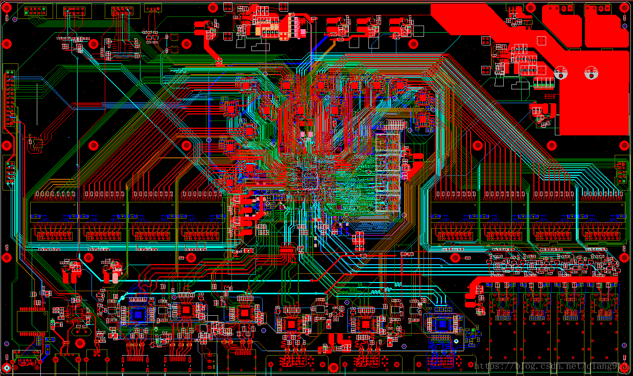
With the increasing demand for high-speed digital systems (e.g., 5G, AI processors, and high-frequency networking), PCB design has become more complex. Ensuring signal integrity (SI), power integrity (PI), and electromagnetic compatibility (EMC) requires careful attention to manufacturing and design processes.
This blog explores the critical process considerations for high-speed PCB design, helping engineers optimize performance while minimizing signal degradation.
1. Material Selection: The Foundation of High-Speed PCBs
Key Factors:
(1) Dielectric Constant (Dk) and Loss Tangent (Df):
Low-loss materials (e.g., Rogers, Isola FR408HR) reduce signal attenuation.
Standard FR-4 may not be suitable for frequencies > 5 GHz.
(2) Glass Weave Style
Tight weaves (e.g., spread glass) minimize impedance variations.
(3) Thermal Stability:
High Tg (Glass Transition Temperature) materials prevent warping under heat.
Recommendation:
Use low-Dk/Df laminates for RF and high-speed digital designs.
Avoid cheap FR-4 for multi-GHz applications.
2. Controlled Impedance and Stackup Design
Why It Matters:
High-speed signals require consistent impedance to prevent reflections and signal distortion.
Critical Considerations:
(1) Impedance Matching:
Trace width, spacing, and dielectric thickness must be precisely controlled.
Common standards: 50Ω (single-ended), 100Ω (differential pairs).
(2) Layer Stackup:
Use symmetrical stackups to avoid warping.
Place high-speed signals between ground/power planes for shielding.
(3) Microstrip vs. Stripline Routing:
Microstrip (outer layers): Faster but more susceptible to noise.
Stripline (inner layers): Better EMI shielding but higher loss.
Best Practices:
Simulate impedance using tools like Polar SI9000 before fabrication.
Work closely with your PCB manufacturer to verify stackup tolerances.
3. Signal Routing and Crosstalk Mitigation
Challenges in High-Speed Routing:
(1) Signal Skew: Mismatched trace lengths cause timing errors.
(2) Crosstalk: Adjacent traces induce unwanted noise.
(3) Return Path Discontinuities: Gaps in reference planes increase EMI.
Solutions:
(1)Differential Pair Routing:
Maintain consistent spacing and length matching (e.g., serpentine tuning).
(2) 3W Rule: Keep spacing ≥ 3x trace width to reduce crosstalk.
(3) Via Optimization:
Use back-drilling or blind/buried vias to minimize stubs.
Avoid excessive vias in high-speed paths.
Advanced Techniques:
Ground Guard Traces: Isolate sensitive signals.
Via Shielding: Surround high-speed vias with ground vias.
4. Power Integrity and Decoupling Strategies
Why Power Integrity Matters:
High-speed ICs (e.g., FPGAs, CPUs) demand stable power delivery with minimal noise.
Key Techniques:
(1) Low-Impedance Power Planes:
Use thin dielectrics between power and ground planes.
(2) Decoupling Capacitors:
Place multiple small capacitors near IC power pins.
Follow the "Rule of Thumb" (e.g., 0.1μF + 1μF + 10μF combinations).
(3) PDN (Power Delivery Network) Analysis:
Simulate voltage ripple using tools like ANSYS SIwave.
Common Mistakes to Avoid:
Insufficient decoupling capacitor placement.
Large loop inductances in power traces.
5. EMI/EMC Considerations
Sources of EMI in High-Speed PCBs:
(1) High-frequency signal harmonics.
(2) Poor grounding strategies.
(3) Uncontrolled return paths.
Mitigation Strategies:
(1) Proper Grounding:
Use solid ground planes (avoid split planes under high-speed signals).
Implement stitching vias along board edges.
(2) Shielding:
Apply copper pours or metal cans over sensitive circuits.
(3) Edge Rate Control:
Use series termination resistors to reduce signal overshoot.
Testing and Compliance:
Pre-layout and post-layout EMI simulations (e.g., HyperLynx).
FCC/CE certification testing for commercial products.
6. Manufacturing and Assembly Considerations
PCB Fabrication Tolerances:
(1) Impedance Control: Ensure fab house can achieve ±10% tolerance.
(2) Surface Finish:
ENIG/Immersion Silver preferred for high-speed signals (low loss).
Avoid HASL (uneven surface).
Assembly Challenges:
(1) Component Placement:
High-speed ICs should be placed close to connectors to minimize trace length.
(2) Soldering Quality:
Reflow profile must avoid thermal damage to low-loss materials.
DFM (Design for Manufacturing) Tips:
Provide detailed fabrication notes (impedance requirements, material specs).
Avoid acute angles in traces to prevent acid traps.
Conclusion: Best Practices for High-Speed PCB Success
To summarize, designing high-speed PCBs requires:
✔ Careful material selection (low-loss laminates).
✔ Precise impedance control and stackup optimization.
✔ Smart routing techniques (differential pairs, 3W rule).
✔ Robust power integrity and decoupling strategies.
✔ EMI/EMC mitigation (grounding, shielding).
✔ Close collaboration with manufacturers (DFM checks).
By following these guidelines, engineers can achieve reliable, high-performance PCBs for next-gen applications.

Please send Email to kspcba@c-alley.com or call us through +86 13828766801 Or submit your inquiry by online form. Please fill out below form and attach your manufacturing files( PCB Gerber files and BOM List) if need quotation. We will contact you shortly.
 +86 13828766801
 kspcba@c-alley.com
 https://www.kingshengpcba.com/
 2/F, Building 6, Tangtou 3rd Industrial Zone, Tangtou Community, Shiyan Town, Baoan District, Shenzhen, China, 518108
We would also like to thank our customers for their trust and support. The company's outstanding achievements are mainly due to the loyalty of our customers, which also encourages and spurs our company to forge ahead.


