* On your first PCB Assembly order!
* Up to $300 discount
 C - A L L E Y
 Home | Events | PCB | About Us | News | Contact Us
Introduction
The strategic vertical arrangement of signal, power, and ground layers directly governs signal integrity, EMC compliance, thermal stability, and manufacturing scalability.
At KingshengPCBA, we collaborate closely with engineers and procurement specialists to optimize PCB layer stackups, ensuring peak performance, cost efficiency, reliable production, and long-term product success. This guide provides a comprehensive roadmap of key strategies and best practices, from conceptual planning to manufacturing execution.
1. Why Layer Stackup Determines the Success or Failure of High-Speed PCB Designs
Have you ever wondered: Why do some PCBs pass EMI tests effortlessly, while others with identical schematics repeatedly fail?
The answer often lies in the layer stackup.
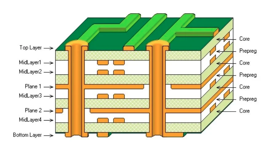
Three Fundamental Roles of Stackup Design:
Ensuring Signal Integrity (SI)
Stackup defines impedance pathways. Poorly arranged layers cause impedance mismatches, signal reflections, jitter, and EMI interference.
High-speed signals require clear return paths via adjacent ground planes—a well-planned stackup guarantees this.
Ensuring Signal Integrity (SI)
EMC success hinges on effective field containment. An optimized stackup strategically confines interlayer electromagnetic fields, creates low-inductance loops, and isolates sensitive signal/power domains, drastically reducing radiation and susceptibility.
Thermal Management
Ground and power planes act as heat sinks. Poor stackups create hotspots, especially around high-power components like regulators and transistors.
Balanced layer distribution ensures even heat dissipation, enhancing PCB reliability.
No schematic or layout, no matter how detailed, can compensate for a suboptimal stackup architecture. From RF signals to USB differential pairs, a PCB’s performance is fundamentally rooted in its layer arrangement.
2. How to Design the Optimal Stackup: A Practical Guide for PCB Designers
Step 1: Align Stackup Decisions with Electrical Intent
Effective PCB stackup design begins not with layer counts or copper weights, but with clearly defined electrical objectives. The stackup must enable your performance envelope—not constrain it. Start by identifying:
(1) Critical parameters (Highest signal frequency, Impedance requirements (e.g.,50Ω single-ended or 100Ω differential), Mixed-signal integration (e.g., sensitive analog front-ends paired with noisy digital logic).)
These above variables dictate trace geometries, plane strategies, and material selection.
Misalignment between stackup planning and electrical goals is a leading cause of:
(2) EMI test failures
(3) Degraded signal integrity
(4) Costly layout rework
Step 2: Prioritize Proximity to Reference Planes
Every signal layer must be adjacent to a well-defined, uninterrupted return plane (typically ground). This ensures:
(1) Low-inductance current return paths (critical for controlled impedance).
(2) Suppression of common-mode noise coupling.
Consequences of poor reference plane management:
(1) High-speed traces without proper reference planes become unintentional antennas.
(2) Transitions across split planes (e.g., beneath differential pairs) introduce:
Mode conversion
Radiated EMI
Timing violations
Key Insight: Stackup design is not just about vertical layer ordering, it's about field control.
Mastering Layer Pairing, Symmetry and Materials
Beyond electrical performance, mechanical symmetry in multilayer PCBs is critical for manufacturability and long-term reliability. In stacks beyond 4 layers, balanced copper weights and dielectric spacing prevent warping, twisting, and lamination defects. Symmetrical mirroring (copper content and dielectric spacing) ensures flatness during lamination, especially under thermal cycling and reflow stress—vital for automotive, aerospace, and industrial applications.
Material selection equally matters:
(1) Standard FR4 suits general use but suffers above 1–2 GHz due to high Df.
(2) High-Tg FR4, Rogers 4350B, or Isola 6 excel in Dk stability, low loss, and thermal reliability—with tradeoffs in cost and process compatibility.
At KingshengPCBA, we co-develop stackups optimized for signal integrity, EMC, and manufacturability, backed by impedance modeling and production validation. Today’s high-speed designs demand stackups tailored to both electrical goals and fab realities—validated with your PCB partner from Day 1.

Please send Email to kspcba@c-alley.com or call us through +86 13828766801 Or submit your inquiry by online form. Please fill out below form and attach your manufacturing files( PCB Gerber files and BOM List) if need quotation. We will contact you shortly.
 +86 13828766801
 kspcba@c-alley.com
 https://www.kingshengpcba.com/
 2/F, Building 6, Tangtou 3rd Industrial Zone, Tangtou Community, Shiyan Town, Baoan District, Shenzhen, China, 518108
We would also like to thank our customers for their trust and support. The company's outstanding achievements are mainly due to the loyalty of our customers, which also encourages and spurs our company to forge ahead.


