* On your first PCB Assembly order!
* Up to $300 discount
 C - A L L E Y
What is Multilayer PCB?
A multilayer PCB contains three or more copper layers. Thus, there can be 3, 4, 5…, 50…, 100, or even more layers. Keep in mind that it is not possible to place the components on all layers of a multilayer PCB, as they can only be placed over the surface layers. The other layers of PCB are used to distribute the connection and wiring between them. The connections are distributed among the layers, which is why complex operations are possible, and connections can be made without wasting the space on the board.
A multilayer printed circuit board (PCB) contains two or more conductive copper layers separated by dielectric material layers such as FR-4. Multilayer PCBs enable increased component density by allowing placement on both sides as well as internally buried layers. They are commonly used in complex digital circuits, RF/microwave systems, high-speed computing, and other applications requiring high interconnectivity.
Compared with single-layer PCB and double-sided PCB, a multi-layer PCB is a printed circuit board with at least three conductive layers. The electrical connection between multilayer printed circuit board layers is realized through plated holes on the circuit board. The number of layers of a Multilayer circuit board can be 4, 6, 8, 10 Up to 100 layers.
More and more PCB manufacturers are involved in the multilayer PCB manufacturing industry, so the manufacturing process and technology have also developed rapidly. Fast turnaround multilayer PCB prototyping and assembly has become a reality.
Multilayer PCB Printed Circuit Board Assembly Process
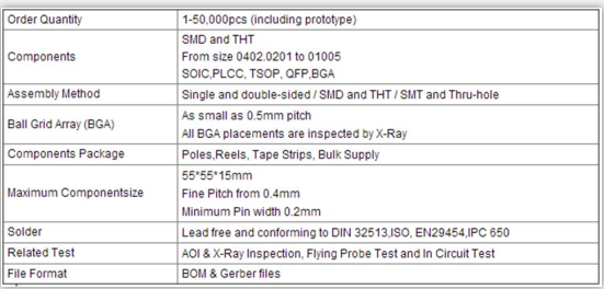
In order to produce multilayer PCBs, the engineering team of the PCB manufacturer will first pre-review and assess the PCB design files—such as Gerber files—provided by the customer. This process will gather information about the number of layers, board thickness, surface finish, solder mask, materials, and other details that correspond to the factory's process capabilities.
Second, alternating prepreg (PP) and core materials are laminated together under high pressure and temperature to create multilayer PCBs. The lamination procedure makes sure that the adhesive holding the layers together is sufficiently melted and cured and that there is no air trapped between the layers.
Many materials can be used to create multilayer printed circuit boards (PCBs); rigid PCBs are made of FR4, high-temperature graphene (HTG) materials, or high-frequency materials, while flexible PCBs are made of polyester or polyimide films.
Fabricating a multilayer PCB requires specialized sequential lamination processes to bond multiple double-sided circuit layers together into a consolidated board. Here are the typical manufacturing steps:
1. Inner Layer Formation
2. Layer Lamination
3. Drill Holes
4. Hole Plating
5. Outer Layer Processing
6. Testing and QA
Why Choose China PCBA Supplier KSPCBA as Your Multilayer PCB Printed Circuit Board Assembly Process Electronics Manufacturer?
– Experienced and skilled team
– State-of-the-art equipment
– Strict quality control
– Excellent customer service
– Competitive price
How can we make high quality PCBA products?
Strict incoming material inspection control and management.
Never change BOM indicated material brand without customer’s permission.
Standard Operation Procedure
PCB will be baked in the oven machine in advance.
Fully automatic, high precision SMT and test equipment.
Comprehensive testing include AOI,X-Ray,ICT,software burning according to different PCBAs.
Strict quality management system.
Please send Email to kspcba@c-alley.com or call us through +86 13828766801 Or submit your inquiry by online form. Please fill out below form and attach your manufacturing files( PCB Gerber files and BOM List) if need quotation. We will contact you shortly.
 +86 13828766801
 kspcba@c-alley.com
 https://www.kingshengpcba.com/
 2/F, Building 6, Tangtou 3rd Industrial Zone, Tangtou Community, Shiyan Town, Baoan District, Shenzhen, China, 518108
We would also like to thank our customers for their trust and support. The company's outstanding achievements are mainly due to the loyalty of our customers, which also encourages and spurs our company to forge ahead.
