We have trusted experts in multilayer PCB design and manufacturing. With our expertise and advanced capabilities catering to a wide range of industries and applications.
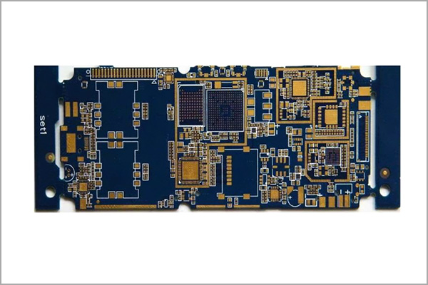
Any circuit board that is more than or equal to 2 layers can be called a multi-layer circuit board, such as 4 layers,6 layers, or 8 layers etc pcb board, Multi-layer circuit board can be divided into,multi-layer rigid circuit board,multi-layer flexible circuit board,multi-layer flex-rigid circuit board.
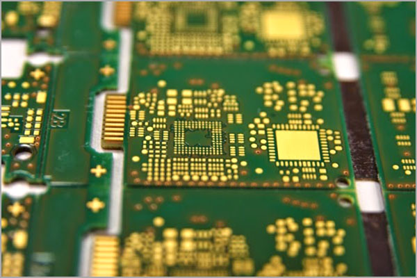
Double-sided PCB, has a dielectric layer in the middle of the layer, and both sides are trace layers, but the multilayer PCB board is a multi-layer trace, and a dielectric layer between each two layers, and the dielectric layer can be made very thin.
Multilayer PCB boards are manufactured by stacking two or more circuits on each other with reliable pre-set interconnections, the production method is generally made by the inner layer pattern first, and then made into a single or double-sided substrate by a printing etching method, which is incorporated into the specified layer, and then heated, pressed and bonded, the subsequent drilling is the same as the plated through-hole method for the double layers PCB.
In principle, the multi-layer circuit board can be made with as many layers as possible, as long as the equipment capacity can be achieved, but in fact, the most common Multilayer PCB is 4-10 layers, special PCBs can be more than 100 layers, but this is not suitable for mass production, the common prototype or mass production multilayer PCB is 4~10 layers PCB.
The increase in circuit package density leads to a high concentration of interconnect lines, which makes the use of Multi-layer PCB necessary.
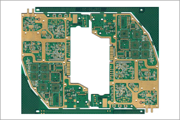
Multilayer printed circuit is the product of electronic technology developing towards high speed, multi-function, large capacity, and small volume, with the continuous development of electronic technology, especially the extensive and in-depth application of large-scale and ultra-large-scale integrated circuits, multi-layer printed circuits are rapidly developing into high-density, high-precision, high-level digitalization, with fine lines and small apertures, blind hole buried holes, and other technologies to meet the needs of the market.
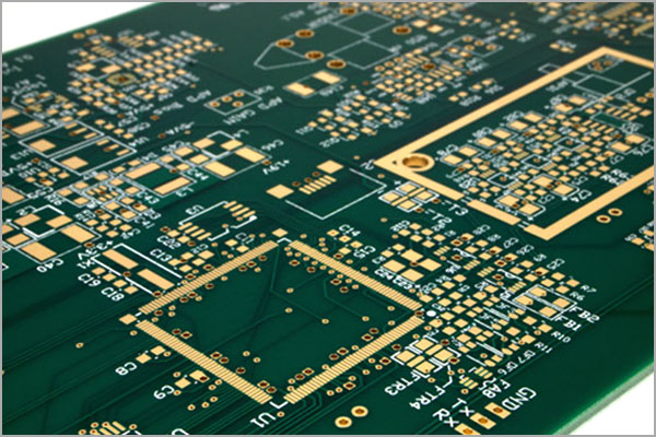
Advantages of multilayer circuit board: high assembly density, small volume, lightweight due to high assembly density, the connection between each component (including components) reduced, to improve the reliability, the number of wiring layers can be increased, thereby increasing design flexibility, it can form a circuit with a certain impedance and a high-speed transmission circuit, it is easy to install and has high reliability.
PCB industry prospects: the market for PCB circuit boards is constantly evolving. First, the market space for the application of the PCB circuit board continues to expand, with the improvement of application in the communication industry, as a result, the market of high-end multi-layer PCB circuit boards grows rapidly. On the other hand, due to the fierce competition in the PCB industry, some large PCB manufacturers like us actively develop new technologies, increase the number of PCB layers or promote the marketization process of FPC with high technical requirements to meet the changing market demand.
Key features of our manufacturing capabilities:
Multilayer PCB fabrication up to 60 layers
Advanced material options, including FR-4, high-frequency and specialized substrates
Controlled impedance and high-speed design support
Blind and buried vias, via-in-pad, and micro-via technology
Fine-pitch component assembly and advanced soldering techniques
ROHS compliant and lead-free manufacturing options
Comprehensive testing and inspection, including electrical testing, AOI, and X-ray inspection
Schematic capture and layout design
Signal integrity analysis
Component selection and BOM optimization
Design for manufacturing ability (DFM) and design for test ability (DFT)
Thermal management solutions
High-speed and impedance-controlled design
Manufacturing Capabilities
We boast state-of-the-art manufacturing facilities equipped with advanced equipment and technologies to ensure the highest quality and precision
In multilayer PCB fabrication. Our manufacturing processes adhere to industry standards and undergo rigorous quality control measures at every stage.
Please send Email to kspcba@c-alley.com or call us through +86 13828766801 Or submit your inquiry by online form. Please fill out below form and attach your manufacturing files( PCB Gerber files and BOM List) if need quotation. We will contact you shortly.
 +86 13828766801
 kspcba@c-alley.com
 https://www.kingshengpcba.com/
 2/F, Building 6, Tangtou 3rd Industrial Zone, Tangtou Community, Shiyan Town, Baoan District, Shenzhen, China, 518108
We would also like to thank our customers for their trust and support. The company's outstanding achievements are mainly due to the loyalty of our customers, which also encourages and spurs our company to forge ahead.


