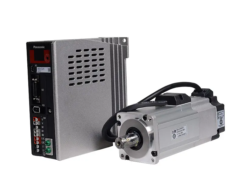
Key Design Pain Points and Solutions for Industrial Servo Motor Driver PCBA
As the core power control unit of automation equipment, the industrial servo motor driver presents multiple technical challenges in
PCBA design, including high power density, high current carrying capacity, high-frequency PWM signal integrity, and precision sampling accuracy. Based on actual production data, traditional contract manufacturers that directly launch production using only Gerber files often achieve a mass production yield of only around 85% for
servo driver PCBAs. Furthermore, more than half of field failures at customer sites are directly related to PCB layout design defects. This article, grounded in the front-end design review and process optimization experience of a
PCBA manufacturing facility, outlines the primary design pain points for servo driver PCBAs and provides verified systematic solutions.
 I. High/Low Voltage Isolation and High-Frequency Interference Suppression
1.1 Pain Point Analysis
I. High/Low Voltage Isolation and High-Frequency Interference Suppression
1.1 Pain Point Analysis
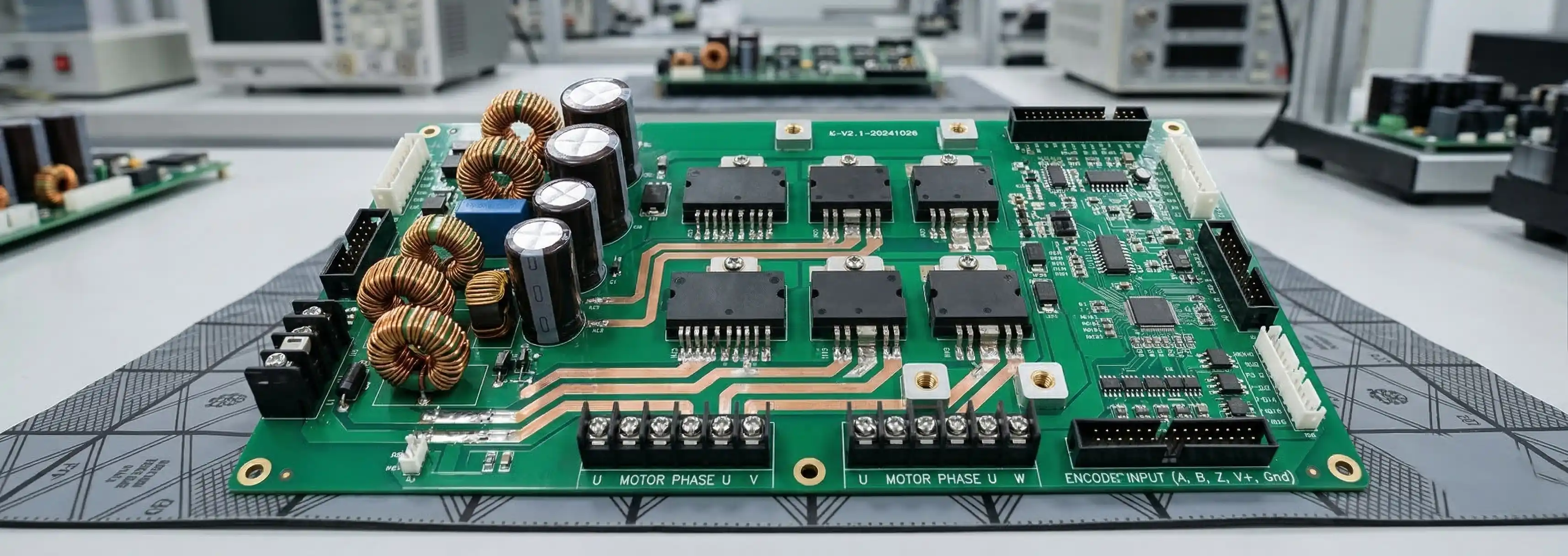
Two fundamentally different circuit types exist within a servo driver: the power circuit carrying PWM switching currents and the precision signal circuit handling encoder feedback. Actual design reviews have revealed that some engineers place PWM routing and encoder signal lines in parallel with a spacing of only 3mm. In an environment with a 20kHz PWM switching frequency and a dv/dt peak reaching 10kV/μs, this distance fails to provide effective isolation. The resulting high-frequency common-mode noise couples into the signal channel through parasitic capacitance, manifesting as low-frequency motor jitter or excessive terminal positioning inaccuracies.
1.2 Solution
During operations, a strict partitioning strategy separating high-current and low-signal sections is mandatory. The layout of power devices and control chips must be clearly divided into physical zones. The spacing between PWM routing and encoder feedback signal lines must be forcibly increased to over 8mm. An isolation strip, no less than 3mm wide, should be placed between them. This strip connects to the main ground plane with low impedance via an array of vias. For high-speed signals like encoder feedback, forced differential pair routing is required, with a controlled differential impedance of 100Ω ±5%. An RC filter network (1kΩ resistor + 0.1μF capacitor) and a 600Ω@100MHz ferrite bead should be added in parallel at the receiving end, suppressing coupled noise from 200mVpp to below 15mVpp.
II. Current Sampling Accuracy and Temperature Drift Control
2.1 Pain Point Analysis
Vector control algorithms demand extremely high accuracy for phase current sampling, with error limits typically set at ±0.5%. However, in mass production, high sampling error dispersion is a prominent issue. Two primary root causes exist. First, the distance between the shunt resistor and the ADC input is too long (exceeding 8cm), allowing high-frequency transient currents to induce millivolt-level voltage spikes on the long path. Second, standard resistors have high temperature coefficients (TCR), reaching up to ±100ppm/℃. In conditions affected by power device temperature rise, with an ambient temperature of 60℃, sampling errors can expand to ±3%.
2.2 Solution
From the manufacturing perspective, using a high-precision shunt resistor with a four-terminal Kelvin connection structure (e.g., the Vishay Z-Foil series with a TCR as low as ±0.2ppm/℃) is mandatory. For the layout, the physical distance between the shunt resistor and the ADC conversion chip should be limited to no more than 3cm, with the trace following a shortest-path principle. Topologically, adding a first-stage RC filter (1kΩ + 0.1μF) and a series ferrite bead at the ADC front end severs the path for high-frequency noise into the sampling channel. To address temperature rise, integrating an NTC thermistor or a TMP102 digital temperature sensor near the power transistors is recommended. The main control chip can read the real-time temperature to perform software compensation on the sampling results. Practical measurement shows this method stabilizes the full-temperature-range error within ±0.1%.
 III. Power Density vs. Thermal Management Conflict
3.1 Pain Point Analysis
III. Power Density vs. Thermal Management Conflict
3.1 Pain Point Analysis
Achieving miniaturization, servo drivers generally aim for high power density (target >50W/in³). However, on a limited PCBA area, power devices (IGBTs/MOSFETs) generate significant Joule heat during high-current (peak 20A-50A) conduction and high-frequency switching. Relying only on standard 1oz copper thickness and natural convection cooling can easily cause MOSFET junction temperatures to exceed the 125°C safety threshold, triggering thermal shutdowns or accelerating fatigue cracking of solder joints.
3.2 Solution
A strategy combining thick copper and multi-layer stacking should be implemented for the power circuit. The main current-carrying circuit should use a minimum copper thickness of 2oz, increasing to 3oz in areas with severe local heating around the power device pads. This reduces the DC resistance (DCR) and, consequently, the I²R losses. Thermally, a dense array of thermal vias (0.3mm diameter, 1mm pitch) should be placed under the thermal pads of the power devices. This array penetrates the entire PCB thickness, conducting heat directly to a dedicated heatsink or aluminum housing on the bottom side. If space is limited, a stacked PCB architecture can be used, separating the power board, driver board, and control board, with the power board specifically constructed on an aluminum-core substrate for enhanced heat dissipation.
IV. Manufacturing Yield Risks and Assembly Concerns
4.1 Pain Point Analysis
Servo drivers often contain precision shunt resistors for current sensing and BGAs for the main control chip. Ignoring manufacturing tolerances during the PCB design phase leads to defects in mass production. Typical issues include: voiding or insufficient wetting of large, thick-copper pads due to uneven heat absorption during
reflow soldering; and solder paste printing defects (insufficient paste) or excessive voiding rates (exceeding 25%) for 0.3mm-pitch BGAs due to improper stencil design, directly reducing high-temperature operational reliability.
4.2 Solution
During the Design for Manufacturing (DFM) review, a critical focus must be placed on matching pad and stencil designs. For thick-copper pads, a stepped stencil should be used to increase the printed solder paste thickness, compensating for the heat absorption effect. For BGA devices, a laser-cut stencil with smooth aperture walls is necessary. Combined with Solder Paste Inspection (SPI), the printing accuracy must be controlled to within ±10μm. For soldering, a reflow profile with a peak temperature of 245°C and a time above liquidus of 60 seconds should be set, balancing joint integrity with device thermal limits. In mass production, X-Ray inline inspection (with a 5% sampling rate on first articles) is mandatory to ensure BGA voiding rates are kept within the
IPC Class 3 requirement of 25%.
Conclusion
The core design pain points for industrial servo motor driver PCBAs lie in three key areas: high/low voltage isolation, thermal management, and sampling accuracy. Proactively intervening during the design phase to identify isolation spacing and thermal via issues, and implementing process controls for thick copper and precision soldering, is the critical path to driving mass production yield from 85% up to and beyond 99%.
 +86 13828766801
 kspcba@c-alley.com
 https://www.kingshengpcba.com/
 2/F, Building 6, Tangtou 3rd Industrial Zone, Tangtou Community, Shiyan Town, Baoan District, Shenzhen, China, 518108


