Defibrillator Mainboard PCBA: Key Design Pain Points and Manufacturing Countermeasures
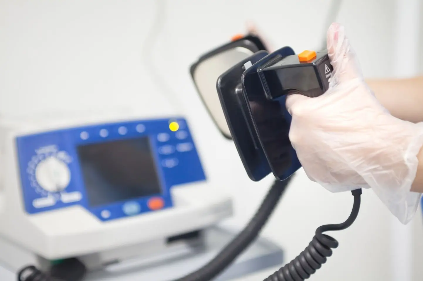
As a life-support device used in emergency scenarios, a defibrillator's mainboard PCBA carries three core functions: high-voltage charge/discharge control, ECG signal acquisition, and system logic control. From a manufacturing perspective, these boards face unique challenges. The same circuit board contains a discharge loop exceeding 3000V and a microvolt-level ECG signal acquisition channel. A high-voltage pulse can break down insulation and damage devices within milliseconds, while radio frequency interference can completely drown out vital sign signals. For a
PCBA assembly factory, understanding and solving these design pain points is a prerequisite for achieving
medical-grade manufacturing reliability.
 I. Isolation Design Pain Points for High-Voltage Discharge and Sensitive Signals
1.1 Pain Point: Mixed Layout of High- and Low-Voltage Circuits Causes Crosstalk and Failure
I. Isolation Design Pain Points for High-Voltage Discharge and Sensitive Signals
1.1 Pain Point: Mixed Layout of High- and Low-Voltage Circuits Causes Crosstalk and Failure
A defibrillator mainboard must simultaneously handle high-voltage charge/discharge circuits (relays, storage capacitors, discharge resistors) and low-voltage signal acquisition circuits (ECG front-end, microcontroller, communication modules). In traditional single-board layouts where the two circuit types are mixed, the electromagnetic radiation generated during high-voltage discharge enters the signal side through spatial coupling and ground loops. This results in ECG amplifier saturation, baseline drift, and even device damage.
1.2 Solution: Physical Isolation and Stacked Architecture
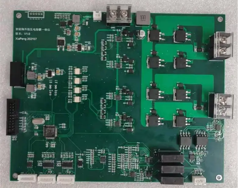
Implement a stacked design separating high and low voltage: Place the low-voltage circuit section and high-voltage circuit section on two separate PCBs and assemble them into a three-dimensional module through stacking. The low-voltage board carries the main controller, standby power supply, and signal acquisition circuits. The high-voltage board concentrates relays, transformers, and internal discharge resistors. Maintain sufficient physical spacing between the two boards or add a grounded shielding layer, ensuring that the high-side reference ground and the low-voltage signal ground are completely independent, thereby blocking crosstalk paths.
Optimize component placement: Mount internal discharge resistors on the high-voltage board with clearance. Reserve space between the resistor body and the board surface. Use this space to accommodate small transformers and similar components, reducing footprint while increasing creepage distance between the high-voltage loop and adjacent circuits.
II. Pain Points in Creepage Distance, Insulation, and Withstand Voltage
2.1 Pain Point: Insufficient Creepage Distance Leads to High-Voltage Breakdown
IEC 60601 standards impose stringent spacing requirements on defibrillator high-voltage circuits. Between live parts of defibrillator electrodes and the handle, creepage distance must reach 50mm and clearance 25mm. Insulation spacing between high-voltage circuits and other circuits must be at least 3mm/kV. Conventional PCB designs often compress spacing in pursuit of miniaturization, leading to failed withstand voltage tests or long-term insulation degradation.
2.2 Solution: Enforced Spacing Rules and Reinforced Insulation
Enforce strict creepage distance rules: In the PCB layout phase, mandate that spacing between all high-voltage nets (storage capacitor positive terminal, relay contacts, discharge loops) and low-voltage nets or mechanical enclosure must not fall below the limits specified in IEC 60601-201 Table 8. For positions where air clearance cannot be satisfied, implement slotting techniques, using air as supplementary insulation.
Select high-insulation substrate materials: Use FR4 Hi-Tg (Tg >170°C) or polyimide substrates, which offer higher dielectric strength than standard FR4 and can withstand high-voltage impulses above 5000V. For critical isolation areas (such as between primary and secondary windings of a transformer), install insulation barriers or use triple-insulated wire.
 III. Pain Points in EMC and Defibrillation Protection for Component Selection
3.1 Pain Point: High-Voltage Pulse Coupling Causes System Reset
III. Pain Points in EMC and Defibrillation Protection for Component Selection
3.1 Pain Point: High-Voltage Pulse Coupling Causes System Reset
During defibrillator discharge, the radiated field strength can reach tens of V/m with wideband characteristics. This pulse couples into the MCU reset pin or power management circuit via power lines, signal cables, or spatial coupling, causing erroneous control system behavior, incorrect discharge timing, or system lock-up. Additionally, defibrillation voltage can back-flow into the device through patient connection ports, damaging the ECG front-end.
3.2 Solution: Graded Protection and Filtering Networks
Patient port protection: Connect low-capacitance TVS diodes (such as ESD5V0D8B) between the ECG lead wires and ground to clamp common-mode pulses to safe levels. The junction capacitance of the TVS must be below 10pF to avoid attenuating ECG signal frequency components. For interfaces such as defibrillator paddle discharge buttons, use TVS arrays with nanosecond response times.
Power entry protection: Configure the AC220V power input port with varistors (20D561K) in series with surge protectors to absorb lightning surges above 3kA. For portable AED battery inputs, use bidirectional TVS diodes (SMDJ24CA) to suppress overvoltage.
Control system hardening: Shunt TVS diodes and ferrite beads across MCU power supply pins. Add single-line protection devices to reset pins to ensure clamping voltage stays below the MCU's absolute maximum rating. Route critical control signal lines as shielded traces with ground surrounds.
IV. Pain Points in Manufacturing Process and Test Verification
4.1 Pain Point: Soldering Defects and Contaminants Cause Long-Term Failure
Medical equipment requires service lives exceeding ten years. However, minor soldering defects (voids, cold joints) or ionic contaminant residues on PCBA can trigger electrochemical migration and CAF (conductive anodic filament) growth under humid and thermal conditions, ultimately leading to insulation failure. Any solder burr or flux residue in the high-voltage region of a defibrillator can become a discharge point.
4.2 Solution: Zero-Defect Manufacturing System
Clean production environment: Perform assembly in a Class 10,000 cleanroom to rigorously control particulate contamination. Use ENIG (electroless nickel immersion gold) or immersion gold finishes for pads to mitigate tin whisker growth risks.
Upgraded inspection methods: In addition to conventional AOI, apply X-ray inspection to high-voltage solder joints to check void rates under BGAs and high-power components (targeting <15%). After assembly, conduct ionic contamination tests to ensure surface cleanliness meets IPC-6012 Class 3 standards.
Reliability validation: Perform HALT and HASS on sampled boards from each batch. Apply thermal cycling (-40°C to 85°C) combined with random vibration to stimulate early latent defects. For high-voltage regions, conduct a 5kV DC withstand voltage test and monitor whether leakage current meets the 500MΩ insulation resistance requirement.
Conclusion
The design and manufacturing of
defibrillator mainboard PCB Assembly essentially involve implementing risk control at the circuit board level. From blocking interference paths through stacked architecture, to ensuring voltage withstand margins with creepage distance and reinforced insulation, to handling pulse impacts with graded protection devices, and finally eliminating soldering risks through zero-defect processes — the rigorous execution at each step ultimately manifests as reliable device activation during critical moments.
 +86 13828766801
 kspcba@c-alley.com
 https://www.kingshengpcba.com/
 2/F, Building 6, Tangtou 3rd Industrial Zone, Tangtou Community, Shiyan Town, Baoan District, Shenzhen, China, 518108


