Autonomous Driving Domain Controller PCBA: Three Major Design Pain Points and Process Countermeasures
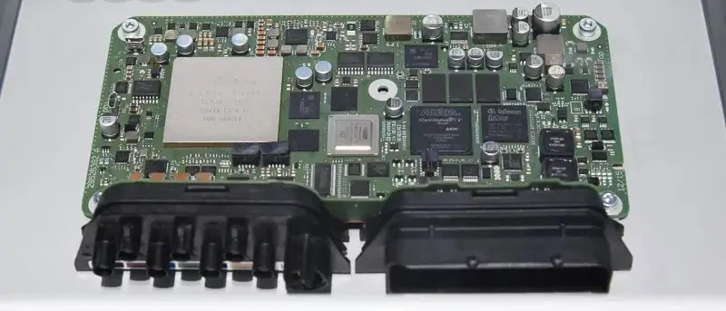
With the evolution of automotive E/E architecture from distributed to centralized, the autonomous driving domain controller has become the core computing unit for L2+ and higher-level intelligent driving systems. This unit integrates high-performance SoCs, AI accelerators, automotive Ethernet switches, multi-channel camera interfaces, and functional safety MCUs on a single
PCBA. The power density of a single board has increased from 2-3W/cm² of traditional ECUs to 8-12W/cm². Meanwhile, the operating environment covers a temperature range from -40℃ to 125℃, the design life requirement is 15 years, and the allowable failure rate is below 0.1ppm. This article describes three types of design pain points in
autonomous driving domain controllers that have the most significant impact on manufacturability and
long-term reliability.
 I. Interrupted Thermal Path Under High Power Density
1.1 Pain Point Description
I. Interrupted Thermal Path Under High Power Density
1.1 Pain Point Description
The power consumption of SoCs in autonomous driving controllers regularly exceeds 100W, with instantaneous peak currents exceeding 100A. However, many designs concentrate high-power devices in a small area while providing insufficient thermal vias under the chips, causing heat to accumulate in inner layers. In one measured case, the AI chip temperature on a domain controller reached 115℃, triggering thermal throttling and causing a 30% loss in computing power. Additionally, automotive-grade MLCC capacitors generate self-heating due to dielectric loss (tanδ > 2.5%) under high-frequency switching scenarios, further elevating local temperatures around the power modules.
1.2 Process Countermeasures
Engineering Specifications for Thermal Vias
Under the thermal pad of power chips, arrange thermal vias with a diameter of 0.3-0.5mm, with a minimum density of 12 vias per cm², and a copper wall thickness of ≥25μm. We require designers to explicitly mark "thermal vias" in Gerber files and specify via filling with resin plugging to prevent solder paste from flowing into the vias, which would cause voids.
Step Copper Thickness Design
Use 4oz thick copper in high-power regions and 1-2oz copper in general signal regions. For thick copper areas, add thief pads to the panel to ensure electroplating uniformity.
Compatible Thermal Interface Material
After SMT placement, attach a thermally conductive gel pad (thermal conductivity ≥3.0W/m·K) on the SoC surface. Maintain compression between 20% and 30% to ensure a continuous heat dissipation path from the PCBA to the housing.
II. Signal Integrity Degradation in High-Speed Links
2.1 Pain Point Description
Domain controllers integrate multiple high-speed buses, including PCIe Gen 4/5 (16-32GT/s), LPDDR5 (6400MT/s), MIPI CSI-2 (8Gbps/lane), and 10GBASE-T1. These signals are highly sensitive to impedance deviation and insertion loss. In production, we frequently encounter three types of issues: first, high-frequency resonance caused by via stubs, which is particularly prominent on links above 10Gbps; second, inadequate control of intra-pair skew – PCIe Gen 4 requires <1ps intra-pair skew, but etching tolerances and glass fiber effects often cause violations; third, power supply ripple coupling into high-speed signal layers, introducing deterministic jitter.
2.2 Process Countermeasures
Standardized Backdrilling
For boards with 10 or more layers, perform backdrilling on PCIe and Ethernet signal vias, keeping stub length within 8mil. Specify backdrilling depth tolerance of ±3mil in process documents and require 100% through-hole inspection.
Low-Loss Laminate Requirements
Standard FR-4 is prohibited. Recommend Panasonic Megtron 6 or Isola I-Speed materials, with dissipation factor (Df) ≤0.005 at 10GHz, to effectively control insertion loss. Confirm the glass fabric style with the laminate supplier, using spread glass or flat glass to minimize the glass fiber effect on differential impedance.
Impedance Coupon Control
Fabricate impedance coupons alongside each production batch and perform TDR testing. Characteristic impedance for 85Ω or 100Ω differential pairs must be controlled within ±8% tolerance (automotive requirements are stricter than consumer electronics' ±10%).
Power Integrity Collaboration
Place multiple 0402-case decoupling capacitors (1nF to 10μF combinations) near the
BGA. During placement, verify capacitor tolerance and temperature rating (X7R or X8R) to suppress PDN high-frequency impedance peaks.
 III. Insufficient Connection Reliability Under Automotive Mechanical Stress
3.1 Pain Point Description
III. Insufficient Connection Reliability Under Automotive Mechanical Stress
3.1 Pain Point Description
Domain controller PCBA installed within the vehicle body undergoes long-term vibration and shock. Three structural weak points frequently cause failures: first, solder joint cracking at the corners of large BGA packages; second, "floating lock" during screw fastening, where the torque specification is met but insufficient clamping force is generated, leading to poor grounding or board warpage; third, broken leads of large electrolytic capacitors or connectors under vibration.
3.2 Process Countermeasures
Mandatory Underfill
For BGAs with 0.4mm pitch or less, and SoCs with dimensions exceeding 20mm, underfill is mandatory. Use capillary-flow underfill material within 24 hours after reflow soldering. The underfill must completely cover the outer four rows of solder balls. After curing, perform a push test; shear strength must exceed 3kgf/mm².
Controlled Screw Fastening Process
Introduce an intelligent tightening system using torque + angle dual monitoring to detect floating lock and cross-threading in real time. For PCBA mounting holes, we recommend adding copper rings at the design stage to prevent substrate cracking during fastening.
Isolation of Stress-Sensitive Components
For large connectors, crystals, and similar components, maintain a minimum distance of 5mm between the component body edge and the board edge or mounting hole. If layout space is constrained, apply corner glue for mechanical reinforcement.

 +86 13828766801
 kspcba@c-alley.com
 https://www.kingshengpcba.com/
 2/F, Building 6, Tangtou 3rd Industrial Zone, Tangtou Community, Shiyan Town, Baoan District, Shenzhen, China, 518108


