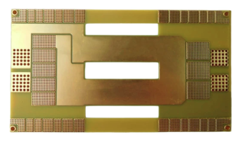
Thick Copper PCB Manufacturing Services
In the age of high-power electronics—where electric vehicles (EVs), industrial motor drives, and renewable energy systems demand robust, current-dense components—standard printed circuit boards (PCBs) often fall short. Thick copper PCBs have emerged as specialized solutions engineered to handle extreme currents, dissipate heat efficiently, and enhance system reliability. At [Your PCBA Factory], we offer end-to-end thick copper PCB manufacturing services, combining advanced plating technologies, rigorous quality control, and expert design support to meet the most demanding industry requirements. This article explores what thick copper PCBs are, how they differ from standard PCBs, their role in reducing EMI and improving signal integrity, and key design guidelines to maximize their performance.
 I: What Are Thick Copper PCBs?
Thick copper PCBs, also called heavy copper PCBs, are defined by their copper foil thickness exceeding the standard 1 oz (35 μm) used in most consumer electronics. Typically, these boards feature copper layers ranging from 2 oz (70 μm) up to 20 oz (700 μm) or more, with custom plating options for ultra-high-power applications. Unlike standard PCBs, which prioritize compactness and cost-effectiveness, thick copper PCBs are built for electrical robustness and thermal performance. They are indispensable for high-power use cases such as EV battery management systems (BMS), solar inverters, industrial power supplies, and welding equipment, where handling large currents and dissipating intense heat are non-negotiable.
II: Standard PCB vs. Thick Copper PCB: Core Differences
The gap between standard PCBs and thick copper PCBs lies in their ability to handle high-power loads and harsh operating conditions. Here’s a breakdown of critical distinctions:
1. Current-Carrying Capacity: A standard 1 oz copper PCB can safely carry 3–5 amps of continuous current per 10mm trace width. In contrast, a 4 oz thick copper PCB handles 12–15 amps under the same conditions—four times the capacity. For EV motor controllers requiring 50+ amps, thick copper PCBs eliminate the need for bulky external busbars, streamlining system design.
2. Thermal Dissipation: Copper has a thermal conductivity of 401 W/mK, far higher than FR-4’s 0.3–0.5 W/mK. Thick copper layers act as integrated heat sinks, rapidly transferring heat from components to the environment. This reduces component junction temperatures by 20–30°C compared to standard PCBs, extending component lifespan by up to 50% and improving long-term reliability.
3. Mechanical Strength: Thick copper adds rigidity to PCBs, making them more resistant to physical shocks, vibrations, and thermal cycling. In industrial environments where equipment faces constant stress, thick copper PCBs maintain structural integrity better than standard boards, reducing solder joint failures and trace cracking risks.
III: How Thick Copper PCBs Reduce EMI and Improve Signal Integrity
Electromagnetic interference (EMI) and signal degradation are major concerns in high-power electronics, where large currents and rapid voltage changes generate unwanted radiation. Thick copper PCBs address these issues through three key mechanisms:
1. Low-Impedance Signal Paths: Thick copper traces have lower electrical resistance than thin standard copper, minimizing signal attenuation and voltage drop over long distances. This ensures high-speed control signals remain intact even in high-current environments. For example, in solar inverters, thick copper traces prevent distortion between microcontrollers and power modules, enabling precise power regulation.
2.Reduced Electromagnetic Radiation: Radiation from traces is proportional to current density. Thick copper allows wider traces at the same current level, lowering density and minimizing radiation. Additionally, thick copper ground planes act as effective shields against external EMI, absorbing unwanted signals and protecting sensitive components from interference.
3. Enhanced Thermal Stability: Heat-induced expansion can warp PCBs, distorting trace geometry and disrupting impedance matching—leading to signal reflection and loss. Thick copper layers have higher thermal mass, reducing temperature fluctuations and minimizing warping. This stable structure maintains consistent impedance, ensuring signal integrity even under extreme thermal conditions.
 IV: Design Guidelines for Thick Copper PCBs
Maximizing thick copper PCB performance requires careful design planning. Our expert engineers recommend these key guidelines:
1.Copper Thickness Selection: Match copper thickness to maximum current and heat dissipation needs. For low-power industrial controls, 2–3 oz copper suffices; for high-power EV components, 6–10 oz may be necessary. Our team provides current density calculations to help you choose optimally.
2. Trace and Pad Design: Use wider traces to reduce current density and heat buildup. Avoid sharp corners on traces, as they create stress points prone to cracking under thermal cycling. Oversize pads to accommodate thick copper layers, ensuring reliable solder joints with heavy components.
3. Layer Stackup Optimization: Place thick copper layers on outer surfaces for maximum heat dissipation, or integrate them as internal ground planes for enhanced EMI shielding. Balance layer thickness to prevent warping during lamination—our factory uses specialized press techniques to minimize distortion even with heavy copper layers.
4. Via and Plating Considerations: Use large-diameter vias to accommodate thick copper plating, ensuring low-resistance layer connections. We offer blind/buried vias and selective plating options to optimize signal paths and reduce unnecessary copper usage.
5. Thermal Management: Pair thick copper PCBs with heat sinks or thermal vias to boost heat dissipation. Our design team simulates thermal performance to identify hotspots and recommends solutions like thermal pads or heat spreaders.
V: At C-alley’s Thick Copper PCB Manufacturing Services
At C-alley, we specialize in manufacturing thick copper PCBs with precise thickness control (±5% tolerance) and uniform plating. Our facilities feature high-current-density electroplating lines that achieve copper thickness up to 20 oz, plus advanced lamination presses to handle heavy layers without warping. We provide full design-for-manufacturability (DFM) analysis to catch issues early, ensuring seamless production and reducing lead times. Our quality control includes ultrasonic thickness testing, impedance measurement, and thermal cycling tests to meet IPC-A-600 and IPC-6012 standards. Whether you need prototypes or large-scale production, we offer flexible solutions tailored to your high-power application needs. Contact us today to leverage our expertise and build reliable, robust electronics

 +86 13828766801
 kspcba@c-alley.com
 https://www.kingshengpcba.com/
 2/F, Building 6, Tangtou 3rd Industrial Zone, Tangtou Community, Shiyan Town, Baoan District, Shenzhen, China, 518108


