RF and Microwave PCBs
In the era of 5G connectivity, autonomous driving, and advanced radar systems, RF (Radio Frequency) and microwave PCBs have emerged as the backbone of high-performance electronic systems. Unlike standard PCBs designed for low-frequency digital or analog circuits, these specialized boards are engineered to transmit and receive signals across the RF spectrum (3 kHz to 300 GHz) and microwave bands (3 GHz to 300 GHz), where signal integrity and minimal loss are non-negotiable. At [Your PCBA Factory], we specialize in manufacturing precision RF and microwave PCBs, offering end-to-end support from material selection to assembly, ensuring our clients get reliable, cost-effective solutions tailored to their high-frequency applications.
 I: What Are RF and Microwave PCBs?
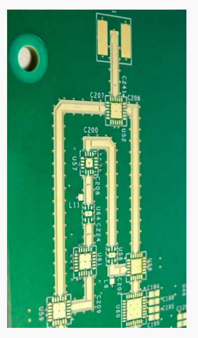
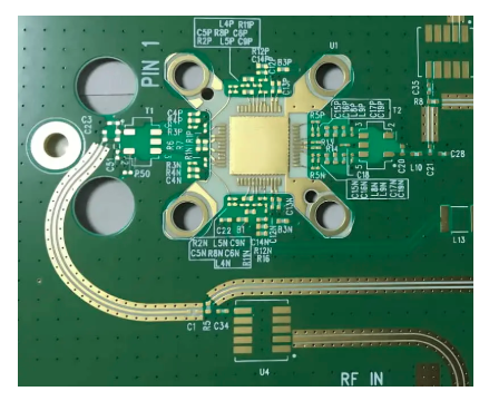
RF and microwave PCBs are specialized printed circuit boards optimized to handle high-frequency signals with minimal attenuation, reflection, and electromagnetic interference (EMI). While RF PCBs cover the broader high-frequency spectrum, microwave PCBs focus specifically on the higher end (3 GHz and above), where signals behave more like waves than traditional electrical currents. The core challenge of these boards is maintaining signal integrity: at high frequencies, signals are prone to loss from dielectric materials, conductor resistance, and radiation, even from small design imperfections. RF and microwave PCBs address this through tailored materials, precise manufacturing, and advanced design techniques, making them critical for applications like 5G base stations, satellite communications, automotive radar, medical imaging, and aerospace systems.
II: Fundamentals of RF and Microwave PCB Design
The performance of RF and microwave PCBs hinges on three core fundamentals that guide every stage of design and manufacturing:
① Low Signal Loss: High-frequency signals lose strength rapidly due to dielectric loss (energy absorbed by the PCB substrate) and conductor loss (resistance in trace materials). Minimizing these losses ensures signals reach their destination with sufficient amplitude for reliable operation.
② Precise Impedance Matching: Impedance mismatch between components and PCB traces causes signal reflection, leading to reduced efficiency and potential signal distortion. RF and microwave PCBs require strict control of trace width, spacing, and substrate thickness to maintain consistent characteristic impedance (typically 50Ω for most RF applications).
③
Robust EMC/EMI Control: High-frequency signals emit electromagnetic radiation that can interfere with other components, while external interference can disrupt signal transmission. Effective shielding, ground plane design, and trace routing are essential to mitigate these risks and comply with industry standards.
III: Critical Materials for RF and Microwave PCBs
The choice of materials is the most influential factor in determining the performance and cost of RF and microwave PCBs. Our factory offers a curated selection of materials to balance performance, cost, and manufacturability:
1.Substrate Materials
The substrate (core material) directly impacts signal loss and stability:
① PTFE (Polytetrafluoroethylene): A fluoropolymer with ultra-low dielectric loss (Df < 0.003) and stable dielectric constant (Dk = 2.2–2.6), ideal for high-frequency applications like radar and satellite communications. Brands like Rogers RO3000 and RT/duroid series are industry standards, though they carry a higher cost due to complex processing requirements.
② Hydrocarbon Resins: These substrates offer a cost-effective balance between performance and affordability, with Df values ranging from 0.008 to 0.015 and stable Dk. Domestic options like Shengyi S7136H provide excellent reliability for 5G base stations and automotive radar, cutting material costs by up to 40% compared to PTFE.
③
PPO/PPE-Based Materials: Modified polyphenylene oxide substrates combine low loss with good mechanical strength, suitable for high-speed digital-RF hybrid circuits used in consumer electronics and industrial RF systems.
2.Conductor Materials
Copper is the standard conductor for RF and microwave PCBs, but high-frequency applications demand specialized options:
① Low-Profile Copper Foil: Reduces skin effect loss (where high-frequency current flows only on the conductor surface) by minimizing surface roughness, ensuring better signal transmission at microwave frequencies.
② Gold-Plated Traces: Offers excellent corrosion resistance and low contact resistance, ideal for high-reliability aerospace applications, though it adds to material costs.
VI: Design Support for RF and Microwave PCBs
Designing RF and microwave PCBs requires specialized expertise, and our team provides comprehensive support to streamline the process and avoid costly reworks:
① DFM (Design for Manufacturability) Analysis: Our engineers review designs early to identify potential manufacturing challenges, such as overly tight trace spacing or incompatible substrate materials. This ensures designs are optimized for our production capabilities, reducing lead times and costs.
② Electromagnetic Simulation: Using tools like ANSYS HFSS and CST Studio Suite, we simulate signal propagation, impedance matching, and EMI/EMC performance before production. This allows us to refine designs to meet performance specifications without expensive prototyping iterations.
③ Impedance Control Guidance: We work with clients to calculate and verify trace dimensions, substrate thickness, and dielectric constants to maintain precise impedance, ensuring minimal signal reflection. ④ Prototype Validation: We offer fast-turn prototyping services, allowing clients to test their designs in real-world conditions. Our prototype runs include full electrical and RF testing to confirm performance before full-scale production.
V: Optimizing Assembly Costs for RF and Microwave PCBs
RF and microwave PCB assembly can be more costly than standard PCBs due to specialized materials and precision requirements, but our cost optimization strategies help clients balance performance and budget:
① Material Selection Consulting: We advise clients on substrate and conductor materials that meet their performance needs without over-specifying. For example, hydrocarbon resins can replace PTFE for mid-frequency applications, cutting material costs significantly while maintaining sufficient performance.
② Process Optimization: Our advanced manufacturing equipment allows us to handle tight tolerances (down to 0.05mm trace width) efficiently, reducing scrap rates and production time. We also optimize panel layouts to maximize material utilization, lowering per-unit costs.
③ Bulk Order Benefits: For high-volume production, we leverage economies of scale to negotiate better material pricing and reduce assembly costs. We also offer flexible production plans to accommodate small-batch prototypes and large-scale runs.
④ Test Cost Reduction: We use automated RF testing equipment to streamline quality control, reducing manual labor costs while ensuring accurate performance validation. For low-volume orders, we offer targeted testing packages to avoid unnecessary expenses.
 VI: Partner with C-alley for RF and Microwave PCB Solutions
As demand for high-frequency electronic systems grows, having a reliable partner for RF and microwave PCB manufacturing is critical. At [Your PCBA Factory], we combine deep technical expertise, state-of-the-art manufacturing capabilities, and client-focused support to deliver high-performance boards tailored to your needs. Whether you’re developing 5G infrastructure, automotive radar, or aerospace systems, we’ll work with you to optimize design, select the right materials, and control costs, ensuring your products meet the highest standards of reliability and efficiency. Contact us today to discuss your RF and microwave PCB requirements..
 +86 13828766801
 kspcba@c-alley.com
 https://www.kingshengpcba.com/
 2/F, Building 6, Tangtou 3rd Industrial Zone, Tangtou Community, Shiyan Town, Baoan District, Shenzhen, China, 518108


