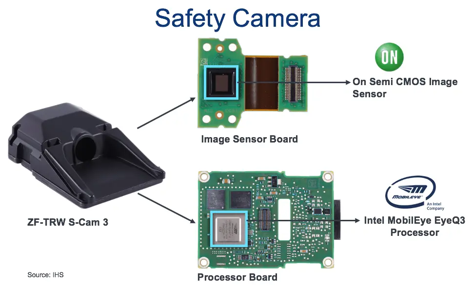
Building ADAS Camera Module PCBA
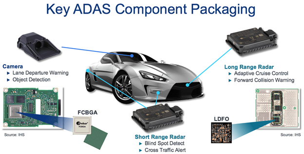
The automotive industry is undergoing its most profound transformation in over a century. As vehicles evolve from mechanical conveyances into intelligent mobile terminals, Advanced Driver Assistance Systems (ADAS) have become the cornerstone of this revolution. Among all ADAS sensors, the forward-looking camera acts as the vehicle's "first eye" – a critical perception component that enables lane keeping, adaptive cruise control, automatic emergency braking (AEB), and traffic sign recognition.
Industry data shows that in the first seven months of 2025, the penetration rate of L2-capable passenger vehicles in China reached 62.58%. With AEB set to become mandatory for new passenger cars in China by 2028, and global L3 conditional autonomous driving permits already being issued, the forward-looking camera market is poised for explosive growth. Global sales of ADAS forward-looking integrated cameras reached US1.075 billionin 2025 and are projected to hit US1.075 billionin 2025 and are projected to hit US2.885 billion by 2032, growing at a CAGR of 15.4%. As a professional PCBA manufacturing facility focused on automotive electronics, we understand exactly what it takes to build a high-performance, ultra-reliable motherboard for these mission-critical modules.
 I. Unprecedented Technical Challenges
Today's forward-looking cameras are rapidly migrating from 2-megapixel to 8-megapixel (8MP) sensors. An 8MP camera generates four times the pixel data per frame, and the entire perception-to-decision loop must complete within 100 milliseconds. This data explosion places extreme demands on the PCBA – from signal integrity to power delivery and thermal management.
Modern architectures typically adopt an "SoC+MCU" dual-core design. The SoC (e.g., Ambarella CV22AQ, Renesas R-Car V4H, or domestic Axera chips) handles visual perception and AI inference, while the MCU manages vehicle-control functions. At the same time, mechanical constraints are severe: the entire camera module is often limited to a footprint of roughly 35mm × 40mm, requiring high-density interconnection (HDI) and micro-miniaturisation. 0.4mm-pitch BGA packages for image sensors demand laser-drilled microvias (approx. 100 μm diameter), via-in-pad filling, and fine-line routing.
High-speed serial interfaces – MIPI CSI-2 running at 1.5 Gbps per lane or more – require meticulous impedance control, differential pair matching, and ground plane continuity. Power management is no less demanding: multiple clean voltage rails for the SoC core, I/O, analog sensor, and SerDes must be delivered by AEC-Q100 qualified PMICs capable of operating from –40°C to +125°C junction temperature, while meeting ASIL B functional safety levels.
II. Overcoming Key Barriers: What It Takes to Manufacture ADAS Camera PCBA
Producing a qualified forward-looking camera motherboard is far beyond conventional consumer electronics assembly. Several formidable barriers separate capable manufacturers from the rest.
1. Automotive-Grade Certification Systems
Entry into the automotive supply chain requires IATF 16949 quality management certification – the basic passport. In addition, PCBA manufacturing must align with ISO 26262 functional safety requirements, and all active and passive components must meet AEC-Q100 and AEC-Q200 standards respectively.
2. Extreme Reliability Demands
The PCBA must function flawlessly across –40°C to +125°C while enduring 10g (10–2000 Hz) vibration. Industry data reveals that non-hardened ADAS HDI PCBs can experience a cracking rate exceeding 25% after only 3,000 thermal cycles. Thus, manufacturers must use high-Tg substrates (Tg≥170℃, such as Shengyi S2116 or Rogers RO4835), maintain blind/buried via copper thickness ≥20 μm, and pass 5,000-cycle AEC-Q200 validation.
3. Precision Manufacturing and Process Control
High-density BGA placement, micro-via plating consistency, and high-frequency impedance control form the "precision triangle". A qualified factory must support 0201/01005 miniature components, laser micro-via drilling, and fully automated optical inspection (AOI), solder paste inspection (SPI), and X-ray inspection. Moreover, a complete MES traceability system is essential to track every batch and process step.
4. Electromagnetic Compatibility (EMC) Design
Excessive EMI is one of the most common bottlenecks during mass production. Split ground planes causing broken return paths, or impedance degradation from plated hole ring variations, can lead to EMC failures and block CISPR 25 certification. Therefore, the factory must possess strong in-house engineering capabilities – not just the ability to follow fabrication drawings.
III. Our Core Competencies: Built for ADAS Forward-Looking Cameras
As a specialised automotive electronics PCBA manufacturer, we have invested years in building the technical foundation and production infrastructure required for ADAS camera motherboards. We offer one-stop service from design review to mass production.
1. Full Automotive Certification – We are IATF 16949 certified and operate under process controls aligned with ISO 26262. From supplier qualification to incoming inspection and FMEA-based process control, every board is manufactured with automotive-grade discipline.
2. Advanced HDI Manufacturing Capability – We master laser-drilled microvias (minimum 0.1 mm), via-in-pad filling and capping, enabling reliable fan-out for 0.4 mm-pitch BGAs. Our SMT lines support 0201 and even smaller components with high precision.
3. Comprehensive Reliability Validation – Each production batch is verified against automotive requirements:
Thermal cycling: –40°C ↔ 125°C, 5,000 cycles
Vibration & mechanical shock: Simulated road conditions
Damp heat: 85°C / 85% RH
100% FCT/ICT: Every board undergoes functional and in-circuit testing before shipment.
4. Full Traceability with MES – Our MES system records everything from material lot numbers to reflow profiles, placement data, and inspection images. Statistical process control (SPC) monitors key parameters in real time, guaranteeing consistency across high-volume production.
5. One-Stop DFM-Driven Service – We provide design for manufacturability (DFM) analysis, component sourcing, PCB fabrication, SMT assembly, DIP, and final integration/testing. DFM review catches potential manufacturing conflicts early – optimising pad geometry, stencil aperture, and reflow profiles to dramatically boost first-pass yield and shorten time-to-market.
 IV. Partner with Us for a Safer Autonomous Future
Every forward-looking camera motherboard we produce carries a profound responsibility – because it directly influences the safety decisions of tomorrow's intelligent vehicles. From 2MP to 8MP, from L2 to L3 autonomy, we are ready to support your journey with proven manufacturing excellence, stringent quality systems, and deep engineering expertise.
Whether you are in the DFM review phase, need stable quality for pilot runs, or demand high efficiency for mass production, we invite you to contact us. Let us build the reliable hardware that makes autonomous driving truly safe and dependable.
Shenzhen Kingsheng Technology Co., Ltd. has rich experience and a professional technical team in PCBA.
Contact KingshengPCBA today to request a quote or discuss your PCBA project.
 +86 13828766801
 kspcba@c-alley.com
 https://www.kingshengpcba.com/
 2/F, Building 6, Tangtou 3rd Industrial Zone, Tangtou Community, Shiyan Town, Baoan District, Shenzhen, China, 518108


