Industrial Barcode Scanner PCBA: A Complete Guide from Design Selection to Production Control
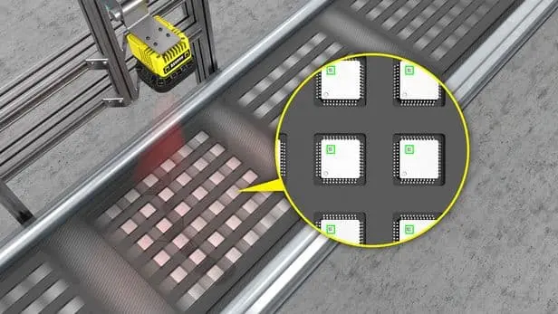
Industrial barcode scanners are core data capture devices in warehousing logistics, production line automation, retail checkout, and similar scenarios. Unlike commercial scanners, industrial-grade products must operate in harsh environments involving high vibration, wide temperature ranges, strong light interference, and dust/water resistance. The PCBA serves as the scanner’s control and signal processing core, directly determining decoding speed, anti-interference capability, and product lifespan. This article, written from the perspective of a PCBA manufacturing facility, outlines the design considerations, component selection rules, key production process control points, and common testing methods for industrial barcode scanner PCBA, providing procurement references for independent station customers.
 I. Core Design Considerations for Industrial Barcode Scanner PCBA
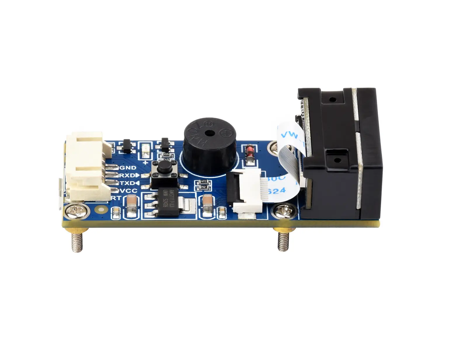
1.1 Image Sensor Interface Layout
I. Core Design Considerations for Industrial Barcode Scanner PCBA
1.1 Image Sensor Interface Layout
Industrial scanners typically use global shutter CMOS sensors to capture high-speed moving barcodes. During PCBA design, the parallel data line length between the sensor and the main control chip should be minimized, with equal-length routing implemented. Differential signal pairs must be strictly impedance-matched to 100Ω. A dedicated ground plane should be placed beneath the sensor to isolate digital noise.
1.2 Decoding Chip and Memory Unit Matching
The mainstream solution uses an ARM Cortex-M7 or M55 core chip with a main frequency not lower than 400MHz. To support decoding algorithms for 1D/2D barcodes (e.g., Code 128, QR code, Data Matrix), at least 16MB of SDRAM and 64MB of Flash must be expanded externally. Flash components must support industrial temperature ranges (-40°C to 85°C).
1.3 Power Supply Topology
Input voltage is typically 5V or 12V. Three independent power rails must be designed: 3.3V for the main control and I/O, 2.8V for the sensor’s analog section, and 1.8V for the core. Each power rail requires ferrite beads and π-type filters. TVS diodes (breakdown voltage 6.5V) are paralleled at critical power nodes to withstand industrial field surges.
1.4 Interfaces and Protection Circuits
- USB 2.0 or RS485 interface: For transmitting decoded data.
- Optically isolated input: Receives external trigger signals, with isolation withstand voltage requirement of 2500Vrms.
- Buzzer drive circuit: Controlled by an N-channel MOSFET to prevent inductive kickback from interfering with the ground plane.
- LED illumination and aiming light control: Independent constant-current driver chip with PWM dimming frequency not lower than 1kHz, eliminating flicker effects on scanning.
II. Key Component Selection Guide
2.1 Sensor and Lens Connector
Recommend using Sony IMX series or onsemi PYTHON series industrial global shutter sensors. The lens holder must use a metal locking connector to prevent focus shift due to vibration. Solder pads for the connector should be reinforced with teardrop pads and vias to enhance mechanical adhesion.
2.2 Passive Component Grade
- Resistors and capacitors: All must be X7R or C0G dielectric; X5R or Y5V is prohibited. Package no smaller than 0603 to reduce placement stress.
- Crystal oscillator: Select industrial grade with ±30ppm temperature drift and apply glue fixing. Load capacitance tolerance 1%.
- Connectors: FPC or pin header connectors interfacing between the scanner and cabling require gold plating thickness ≥0.38μm and insertion/extraction cycle life not less than 500 cycles.
2.3 PCB Material and Process
PCB material: TG170 (glass transition temperature 170°C) or higher FR4, or polyimide flexible board (for bendable scanner guns). Impedance control tolerance ±10%. All vias must be resin-plugged and planarized to prevent ionic migration in humid environments.
III. Key Production Process Control Points for PCBA
3.1 Solder Paste and Printing
Use Type 4 (T4) lead-free solder paste with activity grade ROL0. Stencil thickness 0.12mm, with local thinning to 0.10mm in areas for the sensor and main control chip. Post-printing, 3D SPI inspection must be performed, with solder paste volume tolerance of ±15%.
3.2 Placement and Reflow Soldering
- Image sensor placement: Use a high-precision placement machine (CPK ≥1.33) with pressure control of 50-70g. Reflow must be completed within 2 hours after placement to prevent moisture absorption.
- Reflow profile: Peak temperature 245±3°C, time above liquidus 60-75 seconds. Nitrogen protection with oxygen content below 1000ppm.
3.3 Selective Wave Soldering
For connectors and USB ports in mixed-technology assemblies, conventional wave soldering is prohibited. Selective wave soldering must be used, with preheat temperature 110°C, soldering time 3-5 seconds per point, and solder temperature 280°C.
 IV. Testing Methods and Acceptance Criteria
4.1 In-Circuit Test (ICT)
IV. Testing Methods and Acceptance Criteria
4.1 In-Circuit Test (ICT)
Covers short/open circuit testing, resistor and capacitor value verification, and diode polarity inspection. Test probes must use sharp-pointed tips to penetrate OSP or ENIG surface oxide layers.
4.2 Functional Test (FCT)
Build a dedicated test fixture to simulate industrial field lighting conditions (illuminance adjustable from 0 to 10,000 Lux). Test items include:
- Trigger signal response time ≤10 microseconds.
- Decoding test: Read standard test cards for EAN-13, Code 39, and QR code (version 7), with bit error rate ≤0.01%.
- Communication interface data integrity: Continuously transmit 10,000 data frames with no packet loss or bit errors.
- Illumination light and aiming light intensity and uniformity.
4.3 Aging and Environmental Testing
Sampling test after full PCBA assembly:
- High/low temperature operation: -30°C for 8 hours, then 85°C for 8 hours, power on and decode immediately after each transition.
- Vibration test: 10-500Hz sweep, acceleration 5g, 30 minutes each on X/Y/Z axes. No solder cracks after test.
- Electrostatic discharge test: Contact discharge ±8kV, air discharge ±15kV; PCBA must not restart or freeze.
V. Purchasing and Lead Time Recommendations
For independent station customers purchasing industrial barcode scanner PCBA, note the following:
- Request the PCBA supplier to provide CPK reports, X-ray solder joint inspection images, and aging test records.
- For small pilot runs (50-100 units), prioritize flying probe testing over ICT fixtures to reduce costs.
- For lead times, with all materials available, the PCBA processing cycle is 10-15 working days, including in-circuit/functional testing and 4-hour aging.
- Recommend signing a buffer stock agreement with the PCBA supplier for long-lead-time components such as sensors and main control chips (8-12 weeks), implementing rolling stock replenishment.
Through the end-to-end control chain of design, component selection, production, and testing described above, industrial barcode scanner PCBA can maintain stable decoding performance in harsh environments involving high temperature, vibration, and electrical interference.
Shenzhen Kingsheng Technology Co., Ltd. has rich experience and a professional technical team in PCBA.
Contact KingshengPCBA today to request a quote or discuss your PCBA project.

 +86 13828766801
 kspcba@c-alley.com
 https://www.kingshengpcba.com/
 2/F, Building 6, Tangtou 3rd Industrial Zone, Tangtou Community, Shiyan Town, Baoan District, Shenzhen, China, 518108


