Manufacturing Difficulties of PCBA for 360° Surround View Image Processing Module
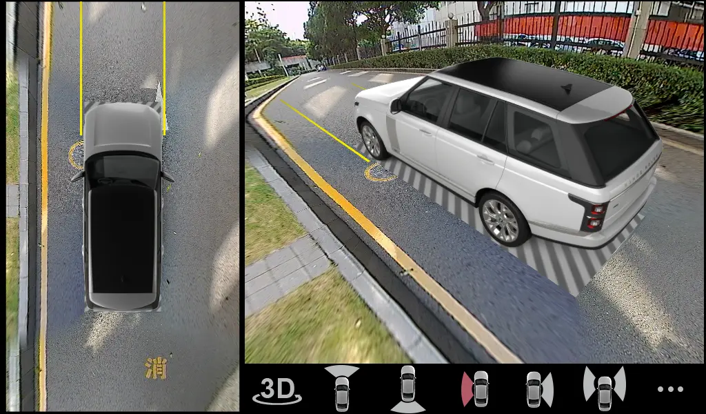
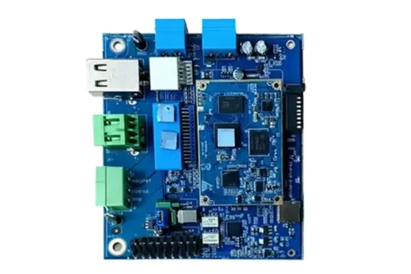
The 360° surround view image processing module is the core component of an automotive panoramic image system. It is responsible for receiving input signals from four or more cameras, performing image distortion correction, stitching and fusion, perspective transformation, and real-time output display. The module is typically based on a high-performance SoC or FPGA solution, integrating DDR memory, a power management unit, a video decoder chip, and various interface protection circuits. Due to the automotive operating environment, the module must meet ISO 26262 functional safety standards and AEC-Q100 grade component selection requirements. The PCBA manufacturing process involves high-density BGA package soldering, impedance control of multiple equal-length signal lines, heat dissipation structure assembly, and automotive-grade reliability verification. The following section analyzes key technical difficulties in manufacturing from five dimensions.
 I. Soldering Process Control for High-Density BGA Packages
1.1 Soldering Risks of Mixed-Size BGAs on the Same Board
I. Soldering Process Control for High-Density BGA Packages
1.1 Soldering Risks of Mixed-Size BGAs on the Same Board
The main control chip of the 360° surround view module often uses a BGA package with a 0.8mm or 0.65mm pitch, while DDR chips and video decoder BGAs are also integrated on the board. The different heat absorption rates of various BGA sizes cause inconsistent temperature rises during the reflow soldering process, easily leading to localized cold joints or bridging. It is necessary to use thermal simulation to determine the temperature curve differences for each BGA area, adopt segmented reflow oven settings, and extend the preheating zone time to over 120 seconds to ensure a ΔT of no more than 5°C within the oven.
1.2 Excessive Void Ratio in Solder Joints
When soldering large BGAs (exceeding 20mm×20mm), the gas generated from flux evaporation is not easily expelled, and the void ratio often exceeds the automotive-grade upper limit of 25%. Solutions include: using a vacuum reflow soldering system to apply a 0.5kPa negative pressure during the solder melting phase; selecting a flux formula with low residue; and optimizing the stencil aperture design using a nine-grid zone exhaust design, keeping the area ratio between 0.68 and 0.72.
II. Length Matching and Impedance Control for High-Speed Signal Lines
2.1 Length Matching Deviation Within DDR Routing Groups
The data groups and address/command groups for DDR4 or LPDDR4 on the module must meet length matching accuracy within ±5mil per group. In actual production, the undercut effect during the etching process causes line width variations, thereby changing the delay per unit length. The manufacturing difficulty lies in maintaining consistent dielectric constant across all DDR signal layers. Laser direct imaging (LDI) exposure equipment is required to control the etching factor above 3. Additionally, time-domain reflectometer (TDR) sampling inspection should be added during the electrical testing phase, and batches with deviations exceeding ±2mil should be compensated and corrected.
2.2 Impedance Fluctuation Between Differential Pairs
The four camera inputs use LVDS or GMSL differential pairs, with a characteristic impedance requirement of 100Ω ± 8Ω. Uneven lamination pressure during the pressing process can cause local variations in dielectric thickness, leading to impedance jumps. During production, impedance test coupons should be monitored every two hours, the resin flow distance of the prepreg should be controlled within 12mm, and a multi-press stepped pressing process should be used to ensure consistent impedance across the entire board.
III. Soldering Reliability Under Automotive Temperature Cycling
3.1 Thermal Cycling Cracking of Ceramic Capacitors
The power filtering circuit of the 360° surround view module uses a large number of X7R or X8R class MLCCs. Automotive temperature cycling test conditions are -40°C to 125°C for 1000 cycles. The difference in coefficient of thermal expansion (CTE) between the MLCC and the FR-4 substrate generates shear stress, easily causing micro-cracks at the capacitor terminations. The manufacturing difficulty lies in selecting flexible termination capacitors and applying underfill reinforcement after placement. The cooling rate during reflow soldering must be controlled between 2°C/sec and 4°C/sec to avoid rapid cooling exacerbating stress.
3.2 Insufficient Thermal Fatigue Life of BGA Solder Joints
BGA solder balls undergo cyclic creep strain during temperature cycling. The grain coarsening of SAC (tin-silver-copper) solder accelerates crack propagation. By using high-reliability solder paste doped with trace amounts of antimony and applying a conformal coating after reflow soldering, the thermal fatigue life of the solder joints can be enhanced to over 1500 cycles. Production requires strict control of solder paste printing thickness deviation within ±10μm to ensure consistency in the volume of all solder joints.
 IV. Cold Solder Joints and Contamination Control for Camera Connectors
4.1 Soldering Misalignment of Micro FAKRA Connectors
IV. Cold Solder Joints and Contamination Control for Camera Connectors
4.1 Soldering Misalignment of Micro FAKRA Connectors
The module is often equipped with four to six micro FAKRA connectors with a pin pitch of 0.6mm. The connector housing softens at high temperatures during reflow. Coupled with uneven placement pressure, this easily results in misalignment between the pins and pads. In production, a fixture with a pressure block is used to apply 150g to 200g of vertical force on each connector. 3D solder paste inspection (SPI) is used to monitor solder paste volume deviation; if deviation exceeds 15%, the line is stopped for adjustment.
4.2 Signal Attenuation Caused by Flux Residue
Flux residue remaining between connector pins can form ionic migration paths in high-humidity environments, increasing insertion loss for high-frequency signals. It is necessary to introduce an in-line plasma cleaning process. After reflow soldering, the connector area is treated with argon plasma for 30 seconds to control ionic contamination below 0.5μg/cm². Conformal coating should be applied within 4 hours after cleaning to prevent recontamination.
V. Mechanical Stress Control During Heat Sink Assembly
5.1 Uneven Compression of Thermal Pad
The top of the module needs to be attached to a heat dissipation aluminum housing. A thickness deviation of the thermal pad exceeding ±0.2mm can lead to locally increased contact thermal resistance. During assembly, use positioning screw posts to control the compression ratio between 25% and 35%. Add inline X-ray inspection to ensure there are no air bubbles in the thermal pad covering the BGA center area. The thermal pad hardness should be selected as Shore OO 30 to 40 to avoid excessive pressure cracking solder joints of adjacent components.
5.2 PCB Warpage Caused by Screw Tightening
The heat dissipation structure uses screws fixed at the four corners. Excessive tightening torque or incorrect sequence can warp the PCB, placing tensile stress on BGA solder joints. In production, use a torque-controlled electric screwdriver set to a limit of 0.3N·m. Follow a diagonal, alternating, stepwise tightening sequence for the screws, with an increment of 0.1N·m per step and a 5-second stress relief interval between steps. After assembly, use a laser flatness measurement instrument to inspect board warpage; the total board warpage must be less than 0.75mm.
Conclusion
The manufacturing of PCBA for the 360° surround view image processing module involves multi-dimensional control of materials, processes, equipment, and inspections. From BGA soldering voids, high-speed signal impedance consistency, temperature cycle solder joint reliability, connector contamination control, to heat sink assembly stress management—each difficulty requires quantified process parameters and the deployment of inline monitoring methods. Only PCBA factories possessing these capabilities can meet the mass production requirements for automotive modules, thereby reducing the field failure rate of the vehicle's panoramic image system.
Shenzhen Kingsheng Technology Co., Ltd. has rich experience and a professional technical team in PCBA.
Contact KingshengPCBA today to request a quote or discuss your PCBA project.
 +86 13828766801
 kspcba@c-alley.com
 https://www.kingshengpcba.com/
 2/F, Building 6, Tangtou 3rd Industrial Zone, Tangtou Community, Shiyan Town, Baoan District, Shenzhen, China, 518108