A Detailed Guide to the Core Applications and Board Specifications of Charging Station PCB Assemblies
With the widespread adoption of new energy electric vehicles, domestic AC charging points and commercial DC charging points have become integral components of the new energy infrastructure. As the control centre of the charging point and the key component for power conversion, safety protection and communication, the PCBA determines the charging stability, safety rating, fast-charging efficiency and service life of the charging point. Charging stations are high-power power electronic devices, and the requirements for the PCBA’s voltage withstand capacity, heat dissipation, current-carrying capacity, electromagnetic interference resistance and flame retardancy rating are far higher than those for ordinary consumer electronics.
 1. Modular Composition of a Charging Station PCBA System
A charging station is composed of multiple PCBA modules working in concert, including the main control board, power drive board, power supply board, metering and data acquisition board, and human-machine interface board. The main control board acts as the ‘brain’ of the charging station, responsible for overall system logic management, charging process control, fault detection, card recognition, and Bluetooth and 4G network communication. It also establishes a protocol handshake with the vehicle’s BMS (Battery Management System) to match the optimal charging voltage and current. The power drive board handles high-power electrical conversion, managing rectification, inversion, MOSFETs and relay switching; it is the module where high current carrying and heat generation are most concentrated. The power supply board converts high-voltage mains power into low-voltage direct current, providing a stable power supply for the control circuitry, display screen and relays. The metering and data acquisition board collects real-time voltage, current and power data to enable billing metering and overload monitoring; the human-machine interface board handles signal processing for the display screen, buttons, indicator lights and QR code scanning module.
2. Environmental Durability Requirements for Outdoor Charging Stations
As charging stations are used outdoors in the open for extended periods, they are exposed to high temperatures, rain, humidity, lightning surges and voltage fluctuations; therefore, the PCBA must possess high voltage resistance, strong heat dissipation, high insulation, resistance to ageing, and protection against moisture, dust and corrosion.
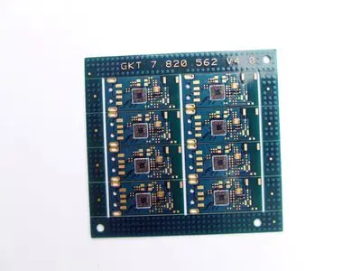
3. PCBA Material and Layer Configuration Standards
Regarding PCBA specifications, the charging station industry adheres to strict standard configurations. The substrate material selected is high Tg, high flame-retardant FR-4, with a Tg temperature of ≥150°C and a flame-retardant rating of V0. It is resistant to high temperatures, minimises delamination and warping, and is suitable for a wide operating temperature range of -30°C to 85°C. In terms of board configuration, low-voltage main control boards and interface boards typically use 2–4-layer PCBs with a thickness of 1.6 mm; high-power driver boards and power supply boards generally employ 4–6-layer thick-copper PCBs, whilst some high-end DC charging stations utilise aluminium-based PCBs to enhance heat dissipation performance.
4. Current-Carrying Capacity and High-Voltage Isolation Design
Current-carrying capacity and copper thickness specifications are particularly critical; signal layers use standard 1 oz copper foil, whilst high-power routing areas employ 2 oz–4 oz thickened copper foil, capable of withstanding high-current long-term loads and reducing circuit heating and voltage drop. The layout employs a design that isolates high-voltage and low-voltage circuits, with physical separation between high- and low-voltage circuits and provision of safety creepage distances to prevent high-voltage crosstalk breakdown. The minimum trace width and spacing is 0.12 mm, with high-voltage traces widened and thickened to enhance insulation and voltage withstand capability.
5. Surface Treatment, Protective Coating and Safety Circuits
Surface treatment typically involves tin plating or electroless gold plating, resulting in secure solder joints with strong resistance to oxidation, making them suitable for long-term, continuous operation. All outdoor charging station PCBs are coated with a triple-proof varnish prior to leaving the factory, providing protection against moisture, dust, salt spray and mould, and effectively withstanding rain, snow, damp industrial sites and corrosive coastal environments. Additionally, the circuitry incorporates overvoltage, overcurrent, earth leakage, lightning protection and emergency shutdown circuits; utilising the PCB’s precision routing to achieve millisecond-level fault disconnection, ensuring the safety of both people and vehicles during charging.
6. Future Development Trends in Charging Station PCBA
Today, charging stations are evolving towards high-power ultra-fast charging, smart networking, shared billing, and secure intelligent operation and maintenance, placing higher demands on PCBA integration, high-frequency interference resistance, high-power heat dissipation, and miniaturised design. Thick-copper multilayer boards, aluminium-based heat sinks, and highly insulated, highly reliable PCBs have become industry standards.
In summary, PCBA serves as the cornerstone for the safe and stable operation of charging stations. The grade of the substrate, the layer structure, the copper foil thickness, the heat dissipation process and the isolation design directly determine the charging efficiency, safety protection and service life of the charging station. Strictly regulated PCBA material selection and process standards are a vital guarantee for the reliable quality and long-term operation of new energy charging stations.
Shenzhen Kingsheng Technology Co., Ltd. has rich experience and a professional technical team in PCBA.
Contact KingshengPCBA today to request a quote or discuss your PCBA project.
 +86 13828766801
 kspcba@c-alley.com
 https://www.kingshengpcba.com/
 2/F, Building 6, Tangtou 3rd Industrial Zone, Tangtou Community, Shiyan Town, Baoan District, Shenzhen, China, 518108


