Three Critical Challenges in Manufacturing Ethernet Switch PCBA
Amidst the wave of digitalization, Ethernet switches, as the core hubs of network data transmission, are witnessing a continuous surge in demand and performance requirements. Whether it's enterprise-grade core switches or industrial-grade equipment operating in harsh environments, the internal PCBA (Printed Circuit Board Assembly) serves as the cornerstone that determines the device's performance, stability, and lifespan.
As a professional PCBA assembly factory, we have accumulated extensive hands-on experience while providing motherboard manufacturing services for Ethernet switches to clients worldwide. Today, let's dissect the most technically challenging aspects of manufacturing Ethernet switch PCBA.
 Challenge 1: HDI and Miniature Component Placement Challenges
Modern switches are evolving towards higher port density and faster processing speeds. This directly leads to PCBs populated with more BGA (Ball Grid Array) packages, 01005-sized passive components, and precision connectors.
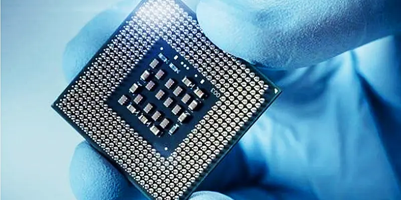
- 1.BGA Soldering and Rework: The main switching chips and PHY chips are typically housed in large BGA packages with fine pin pitches (e.g., 0.8mm or even 0.65mm) and a high ball count. During placement, even slight deviations in solder paste printing release, placement machine pressure, or accuracy can lead to bridging or cold solder joints. More challenging is that even after reflow, controlling the void rate detected by X-Ray inspection remains a significant hurdle. By introducing 3D SPI (Solder Paste Inspection) and optimizing the reflow profile, we ensure the metallurgical structure of BGA solder joints is dense, strictly controlling the void ratio under IPC standards.
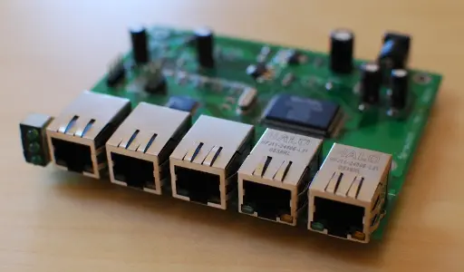
- 2.Precision Connector Placement: RJ45 ports or fiber optic interfaces are typically odd-shaped components with fine pins. Placement not only requires ensuring coplanarity but also preventing displacement during the high temperatures of the reflow process; otherwise, subsequent enclosure assembly becomes impossible.
Challenge 2: Integrity Guarantee and Impedance Control of High-speed Signals
Ethernet switches handle high-frequency signals, such as 10G, 25G, or even 100G. At the level of PCBA manufacturing, how to maintain signal integrity to the greatest extent is the key that distinguishes ordinary processing from precise manufacturing.
- 1.Material and Process Compatibility: High-frequency signals necessitate low-loss PCB substrates (e.g., M4, M6 grades), but these materials are often more brittle and prone to moisture absorption. Under the high temperatures of reflow soldering, there is a high risk of board explosion or delamination. Therefore, we must implement strict pre-baking of PCBs before assembly and design gentler ramp-up rates.
- 2.Consistency in Impedance Control: Differential pairs (e.g., SerDes lanes) in switches are extremely sensitive to impedance. Factors during manufacturing, such as solder mask thickness and copper thickness uniformity, can impact the final characteristic impedance. During processing, we collaborate deeply with the PCB fabricator, precisely calculating and compensating for trace widths based on the final layer stack-up to ensure impedance tolerance is strictly controlled within ±10% or even a tighter ±5%.
Challenge 3: Thermal Management and Power Module Reliability
Switches usually require continuous operation 24/7 and generate a considerable amount of heat. Thermal design involves not only mechanical structure but also the PCBA assembly process.
- 1.Thermal Management for High-Power Components: Main chips and Power Management ICs (PMICs) often require heatsinks. At the PCBA stage, ensuring tight contact between the thermal pad and the chip surface, and achieving uniform clamping pressure from the heatsink, are critical to preventing hot spots and chip damage. We utilize automated pressing and screw driving equipment to guarantee pressure consistency.
- 2.Current Carrying Capacity of Power Modules: PoE (Power over Ethernet) switches need to supply power to powered devices, requiring the high-current paths on the PCBA to have sufficient copper thickness (often 2oz or even 3oz). Thicker copper foils are prone to uneven under-etching or solder mask bubbling during the patterning and solder mask printing processes, posing higher demands on the precision of circuit fabrication.
Conclusion
Manufacturing a high-performance Ethernet switch PCBA is far more than simple component placement. It is a systematic project involving material science, precision mechanical engineering, and thermodynamics. As your manufacturing partner, we are committed to overcoming these technical challenges—from precise BGA placement and rigorous signal integrity testing to efficient thermal assembly solutions—ensuring every shipped PCBA can reliably support the unhindered flow of the data world.
If you are seeking reliable manufacturing support for your next-generation switch products, we welcome you to discuss further technical details with us.
Shenzhen Kingsheng Technology Co., Ltd. has rich experience and a professional technical team in PCBA.
Contact KingshengPCBA today to request a quote or discuss your PCBA project.
 +86 13828766801
 kspcba@c-alley.com
 https://www.kingshengpcba.com/
 2/F, Building 6, Tangtou 3rd Industrial Zone, Tangtou Community, Shiyan Town, Baoan District, Shenzhen, China, 518108


