Decoding the High-Density Integration Challenges of AR Glasses PCBA
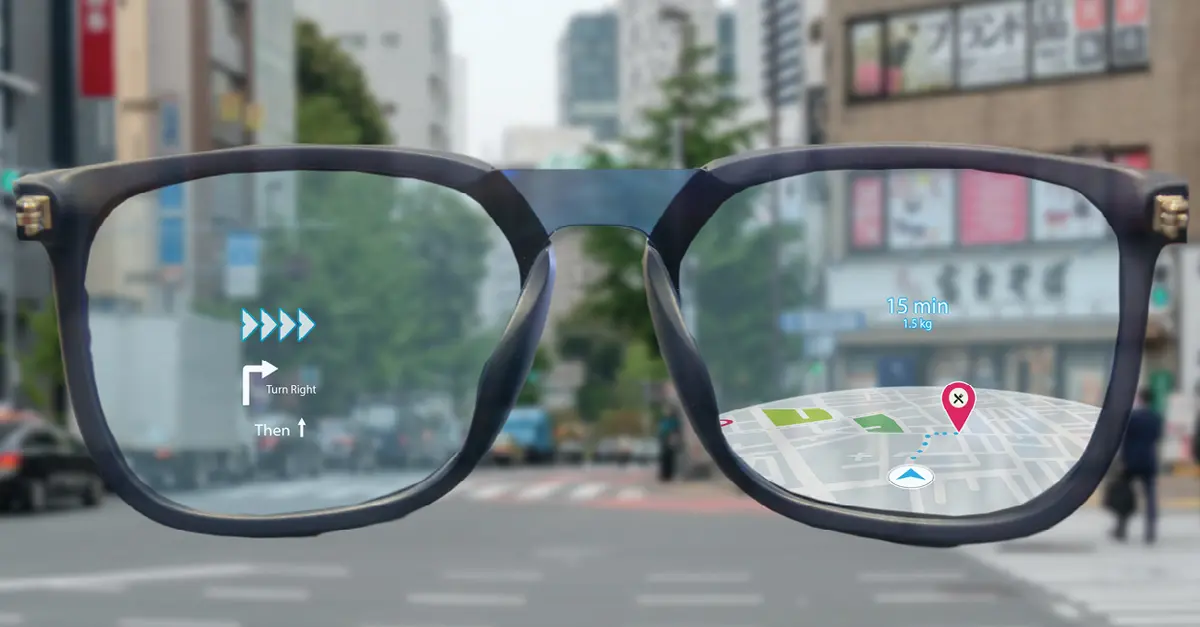
When consumers watch virtual navigation arrows accurately projected onto the real road through a pair of AR glasses, few stop to consider what kind of hardware architecture inside those slender temples is actually supporting this magic. As a technical observer from a PCBA assembly plant, I'd like to approach this from a manufacturing perspective and break down the core technical codes of AR glasses PCBA.
The Routing Under Space Compression

The first major hurdle for AR glasses is volume. Traditional consumer electronics PCBs have ample layout space, but the usable cross-sectional area inside the temples of AR glasses is very limited. To integrate AI processing chips, Bluetooth modules, power management units, camera control circuits, and display drivers within such a cramped space, traditional PCB architectures are simply no longer feasible.
This forces a shift towards High-Density Interconnect (HDI) boards and Rigid-Flex boards. Currently, mainstream AR glasses PCBA commonly employs 6 to 12-layer any-layer HDI structures, with line widths and spacing compressed to within 0.1mm, and even moving towards 50μm. Micro blind and buried vias have replaced through-holes, allowing vertical interconnections between layers without consuming routing channels. Think of it this way: HDI technology is essentially about taking the circuit network that originally needed to be "laid out" and storing it in a small space through a three-dimensional "folding" method.
The Process Limits of Curved Surface Mounting and Irregular Shape Assembly Processes
AR glasses design is shifting from a "flat" to a "fitting" approach. To maximize the use of the quasi-elliptical space inside the temples, and even to accommodate ergonomic curves, the application ratio of curved PCBs and Rigid-Flex boards is rapidly increasing.
However, this presents severe challenges for SMT production lines. When the PCB substrate has flexible properties, the traditional planar mounting coordinate system is no longer fully applicable. Solder paste printing tends to be uneven in thickness on curved areas, and when fine-pitch components flow through reflow soldering, they are prone to displacement or tombstoning due to the difference in the thermal expansion coefficients of the substrates.
The current mainstream industry countermeasures involve laser 3D positioning + dedicated fixture compensation. By scanning to obtain accurate 3D model data of the PCB, the placement machine, when mounting micro resistors/capacitors of size 01005 (0.4mm × 0.2mm) or BGA chips with 0.3mm pitch, must perform real-time dynamic coordinate correction, with placement accuracy consistently controlled within ±25μm. Simultaneously, customized curved adsorption fixtures ensure the board does not deform during the high-temperature soldering zone.
Thermal Management and Reliability
The power consumption paradox of AR glasses is: the stronger the performance, the greater the heat generation, but users absolutely will not tolerate hot temples. Because the internal space is almost entirely filled with components, traditional fan cooling is impossible, PCBA itself must undertake the function of heat dissipation.
This involves multi-level collaboration between materials and processes. Thermoelectric separation design is widely adopted in the design phase, which directly connects the heat dissipation pads of high-heat-generating chips to the inner copper foil or outer copper foil through dense heat sink vias. Some high-end designs incorporate copper coin embedding processes or graphene heat-spreading films to rapidly conduct heat to the frame structure for dissipation.
Furthermore, the usage scenarios for AR glasses are extending from indoors to outdoors. For example, vehicle-mounted AI smart glasses need to withstand wide temperature shocks from -40℃ to 85℃. This imposes stricter reliability requirements on PCBA substrate material selection (e.g., Polyimide), solder joint alloy composition, and Underfill processes compared to standard consumer electronics.
The Future Evolution of Manufacturing
Looking ahead to 2026 and beyond, as Micro LED and diffractive waveguide solutions gradually mature, bandwidth demands on the display driver side will further increase, posing new challenges for PCBA signal integrity design. Simultaneously, as component counts rise, embedded packaging technology—embedding passive components within the PCB's inner layers—is expected to migrate from high-end models towards the mainstream to further free up surface space.
For PCBA manufacturers, while the unit value of AR glasses might not be enormous, they represent a "technical Everest" of precision manufacturing capability. Whoever can pack increasingly complex circuits into increasingly smaller temples will secure an irreplaceable niche in this upcoming wearable interaction revolution.
Shenzhen Kingsheng Technology Co., Ltd. has rich experience and a professional technical team in PCBA.
Contact KingshengPCBA today to request a quote or discuss your PCBA project.
 +86 13828766801
 kspcba@c-alley.com
 https://www.kingshengpcba.com/
 2/F, Building 6, Tangtou 3rd Industrial Zone, Tangtou Community, Shiyan Town, Baoan District, Shenzhen, China, 518108


