How can Low-power Design Be Achieved for Environmental Monitoring Equipment PCBA?
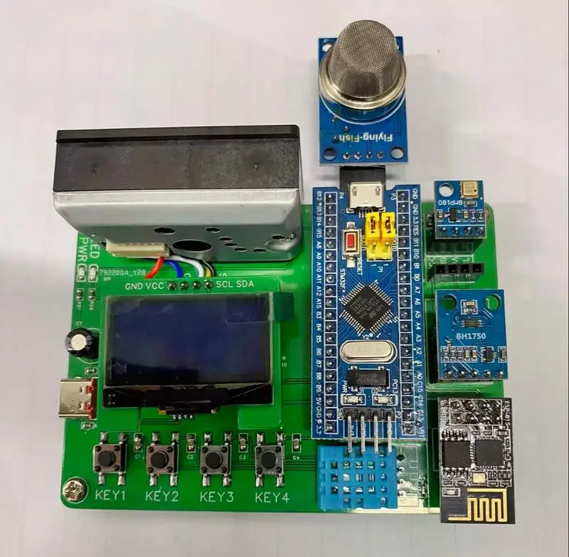
With increasing environmental awareness, environmental monitoring equipment plays an increasingly important role. This equipment typically needs to operate for extended periods, sometimes relying on battery power, making a low-power design of the printed circuit board (PCB) crucial. It not only extends the equipment's lifespan and reduces operating costs but also aligns with the principles of green environmental protection. So, let us talk about how to achieve low-power design for environmental monitoring equipment PCBA from PCB layout and optimization.
Reducing Signal Transmission Loss: For environmental monitoring equipment PCBA, signal transmission loss is converted into heat energy, increasing power consumption. Optimizing PCB layout and routing can reduce signal transmission loss.
Firstly, components should be reasonably laid out, placing closely related modules in proximity to each other to shorten signal transmission paths and reduce signal attenuation during transmission. For instance, sensors should be placed as close as possible to signal processing chips to minimize the length of signal transmission lines. Secondly, when routing high-speed signal lines, appropriate routing methods, such as differential signal routing, should be employed, and the characteristic impedance of the traces should be strictly controlled to ensure signal transmission integrity and reduce energy loss caused by signal reflection. Additionally, avoid excessively long or thin signal lines to prevent increased power consumption due to excessive resistance.

Reducing electromagnetic interference and power consumption correlation:
Electromagnetic interference (EMI) can not only affect the normal operation of equipment but may also be related to power consumption.
In PCB design, take action to reduce electromagnetic interference (EMI), thereby indirectly reducing power consumption. Function areas should be reasonably divided, separating analog and digital circuits to minimize mutual interference. Simultaneously, add shielding measures to circuits susceptible to interference, such as setting up grounded copper foil around sensors to prevent external EMI from affecting the normal operation of the sensors and avoiding increased power consumption due to sensor malfunction caused by interference. Furthermore, through reasonable power and ground layer design, reduce the impact of power supply noise on other circuits, reducing additional power consumption caused by EMI.
Low-power design of PCB for environmental monitoring equipment is a comprehensive task that requires thorough consideration and careful design from multiple perspectives.
Through the effective implementation of these measures, the power consumption of the equipment can be significantly reduced, and the performance and reliability of the equipment can be improved, providing more durable and efficient support for environmental monitoring work.
Shenzhen Kingsheng Technology Co., Ltd. has rich experience and a professional technical team in the field of PCB design and manufacturing for environmental monitoring equipment. We have a deep understanding of the stringent requirements for low power consumption in environmental monitoring equipment and is capable of performing detailed design and optimization.
Contact KingshengPCBA today to request a quote or discuss your PCBA project.
Please send Email to kspcba@c-alley.com or call us through +86 13828766801 Or submit your inquiry by online form. Please fill out below form and attach your manufacturing files( PCB Gerber files and BOM List) if need quotation. We will contact you shortly.
 +86 13828766801
 kspcba@c-alley.com
 https://www.kingshengpcba.com/
 2/F, Building 6, Tangtou 3rd Industrial Zone, Tangtou Community, Shiyan Town, Baoan District, Shenzhen, China, 518108
We would also like to thank our customers for their trust and support. The company's outstanding achievements are mainly due to the loyalty of our customers, which also encourages and spurs our company to forge ahead.


