What are the key points to be noted when designing a communication PCBA?
In the research and development process of communication appliances, PCBA prototyping stage is crucial. Its special design requirements, industry attributes, and the achievement of technical metrics are directly related to the performance, stability, and market competitiveness of communication appliances. Understanding these key points is of great significance to communication appliance manufacturers.
1.Special Design Requirements
(I) High-Speed Signal Transfer Design
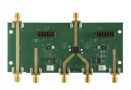
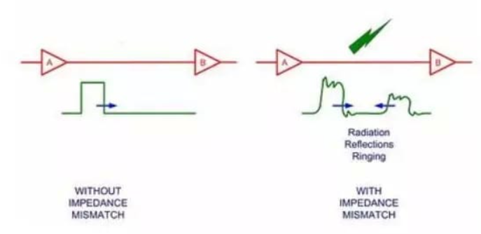
*Line impedance matching: In communication appliances, a large number of high-speed signals are transferred on the PCBA board, such as Ethernet and USB 3.0 interface signals. To ensure signal integrity, it is necessary to precisely control the line impedance. For example, for a transmission line with a characteristic impedance of 50Ω, during PCB layout design, the line parameters should be calculated and adjusted based on factors such as the dielectric constant of the board material, line width, and line spacing through professional software to ensure that the impedance deviation is controlled within a very small range, typically within ±5%.
Otherwise, during the transmission process, the signal will be reflected due to impedance mismatch, resulting in signal distortion and an increase in bit error rate, which seriously affects the communication quality.
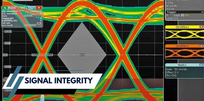
*Signal Integrity Optimization: High-speed signal transmission is prone to interference. Therefore, multiple measures need to be taken to optimize signal integrity, such as shortening the length of signal traces and reducing the number of vias, in order to reduce signal transmission delay and loss. For the critical signals, a shielding method is adopted, that is, by laying ground copper foil around the signal lines, the influence of external electromagnetic interference on the signals is reduced. At the same time, a proper arrangement of the laminated structure of the signal layer, power layer and ground layer should be made. By taking advantage of the shielding effect of the power layer and ground layer, the anti-interference ability of the signal can be further enhanced.
For example, when designing the PCBA board for a high-speed communication module, the signal layer is closely coupled with the adjacent power layer and ground layer, effectively reducing the crosstalk between signals.
(II) Thermal Design
*Heat Dissipation of High-Power Components: High-power components in communication appliances, such as power amplifiers and power management chips, generate a large amount of heat during operation.To ensure the stable operation of the equipment, efficient heat dissipation is necessary. In PCBA design, sufficient heat dissipation space should be reserved for high-power devices. For example, the area of the heat dissipation pads can be increased, and the heat can be conducted to the large-area copper foil on the inner or outer layer of the PCB board through vias. The excellent thermal conductivity of the copper foil is utilized for heat dissipation. For example, in the case of a power amplifier, a large area of heat dissipation pads are designed on the PCB board at its bottom, and these pads are connected to multiple layers of copper foil through dense vias to ensure that the heat can be dissipated quickly.
*Thermal Management System Design: For some communication devices that are sensitive to temperature, such as base station equipment, a comprehensive thermal management system needs to be designed. Besides the aforementioned device-level cooling measures, temperature sensors can also be integrated on the PCBA board to monitor the temperature on the board in real time. Through an intelligent control system, the rotational speed of the cooling fan or the cooling efficiency of the heat sink can be automatically adjusted according to temperature changes. For example, when the temperature sensor detects that the temperature in a certain area of the PCBA board is too high, the control system automatically increases the rotational speed of the cooling fan to enhance the cooling effect and maintain the temperature of the PCBA board within an appropriate range.
(III) Electro Magnetic Compatibility (EMC) Design
*Shielding Design: When communication equipment is operating, it will generate electromagnetic radiation and is also prone to external electromagnetic interference. To reduce the impact of electromagnetic interference on appliance performance, a good shielding design should be conducted. On the PCBA board, for sensitive circuit modules, such as radio frequency modules, metal shielding is adopted for physical shielding. The shielding cover is reliably concatenated with the grounding pins of the PCB board to form a complete shielding cavity, blocking internal radiation leak and preventing external electromagnetic interference from entrance. For example, in the PCBA design of smartphone radio frequency modules, high-precision stamped metal shielding covers are used to ensure the shielding effect.

*Filtering circuit design: Designing filtering circuits at the power input/output ports and signal input/output ports is an important means to elevation EMC performance. By reasonably selecting filtering components such as capacitors and inductors, π-type, T-type and other filtering circuits are composed to filter out high-frequency clutter and interference signals in the power and signal.
For example, at the power enter port of a communication device, a π-type filter circuit is connected in concatenation, which effectively suppresses conducted interference on the power supply cord and warrants stable power supply to the internal circuit of the device.
Please send Email to kspcba@c-alley.com or call us through +86 13828766801 Or submit your inquiry by online form. Please fill out below form and attach your manufacturing files( PCB Gerber files and BOM List) if need quotation. We will contact you shortly.
 +86 13828766801
 kspcba@c-alley.com
 https://www.kingshengpcba.com/
 2/F, Building 6, Tangtou 3rd Industrial Zone, Tangtou Community, Shiyan Town, Baoan District, Shenzhen, China, 518108
We would also like to thank our customers for their trust and support. The company's outstanding achievements are mainly due to the loyalty of our customers, which also encourages and spurs our company to forge ahead.


