* On your first PCB Assembly order!
* Up to $300 discount
 C - A L L E Y

Printed Circuit Board
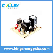
A printed circuit board, or PC board, or PCB, is a non-conductive material with conductive lines printed or etched. Electronic components are mounted on the board and the traces connect the components together to form a working circuit or assembly.
PCB Layout
The art and science of printed circuit board (PCB) layout are deeply entwined with electronics design. From cellphones to spacecraft, PCBs constitute the foundation of many electronic gadgets, and their design and production processes have a big influence on the functionality and dependability of these engineering marvels. We will explore the complex field of PCB layout in detail, illuminating the crucial interactions between solder, PCB manufacturing procedures, stack-up configurations, solder mounts, and board layout as these components come together to form dependable and effective electronic systems.
PCB Copy
PCB cloning, often known as PCB duplication, is a reverse engineering technique used to make duplicates of pre-existing PCBs. It guarantees that you can design the PCB precisely without having to go through the time-consuming design process. For this reason, it is quite efficient in terms of both time and money savings. It is challenging to keep up with the constant evolution of electrical devices using conventional R&D techniques. Thus, reverse engineering is a potent choice. In addition to extending a device's lifespan when its components become outdated, PCB cloning facilitates the modification of pre-existing designs to suit your specific needs.
PCB Design
What is PCB design? Printed circuit board (PCB) design brings your electronic circuits to life in the physical form. Using PCB layout software, the PCB board design process combines component placement and routeing to define electrical connectivity on a manufactured circuit board.
How can we make high quality PCBA products?
Strict incoming material inspection control and management.
Never change BOM indicated material brand without customer’s permission.
Standard Operation Procedure
PCB will be baked in the oven machine in advance.
Fully automatic, high precision SMT and test equipment.
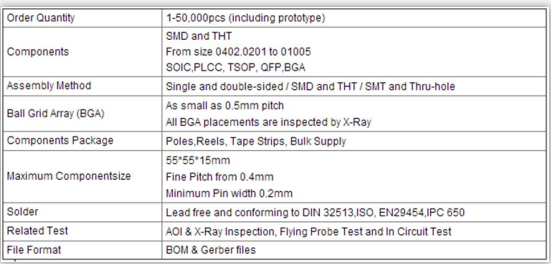
Comprehensive testing include AOI,X-Ray,ICT,software burning according to different PCBAs.
Strict quality management system.

Please send Email to kspcba@c-alley.com or call us through +86 13828766801 Or submit your inquiry by online form. Please fill out below form and attach your manufacturing files( PCB Gerber files and BOM List) if need quotation. We will contact you shortly.
 +86 13828766801
 kspcba@c-alley.com
 https://www.kingshengpcba.com/
 2/F, Building 6, Tangtou 3rd Industrial Zone, Tangtou Community, Shiyan Town, Baoan District, Shenzhen, China, 518108