* On your first PCB Assembly order!
* Up to $300 discount
 C - A L L E Y

What is a PCB?
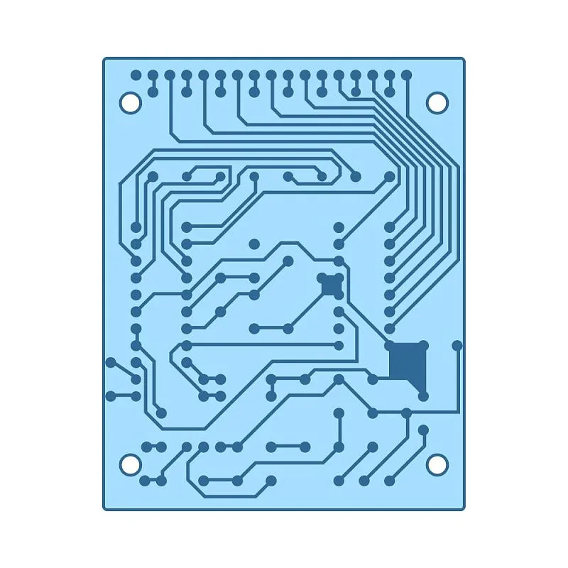
An electronic arrangement known as a printed circuit board (PCB) connects components electrically by use of copper cables. Electronic components are mechanically supported by printed circuit boards, enabling devices to be installed in enclosures. A printed circuit board design needs to follow a certain set of instructions that correspond with the integrated circuit packaging, manufacturing procedure, and bare circuit board structure.
Copper traces, pads, and conductive planes are examples of conductive structures found on printed circuit boards. An insulating material is layered between conductor layers to form the mechanical structure. A silk screen material is printed on top of the non-conductive solder mask, which covers the entire structure and serves as a legend for the electronic components. Following these fabrication stages, the printed circuit board assembly receives the bare board, which is then used to solder components to the board and test the PCBA.
In the electronics business, printed circuit board design has developed into a vertical. PCBs are crucial because they offer sturdy support for holding components in place, electrical connections between components, and a small packaging that can be integrated into a finished device. The greatest software can assist in taking a design from concept to manufacture. Even the most basic circuit board requires careful design utilizing specialized software tools. We'll delve deeper into the definition of a printed circuit board (PCB), its design, and some key concepts to grasp when creating circuit boards in this post.
When it's time to start a new design, printed circuit boards pass through several stages. Production-grade circuit boards are designed using ECAD software, or a CAD application that includes many utilities that are specialized for circuit board design and layout. ECAD software is built to help designers walk through a specific process for circuit board design, beginning with basic electrical drawings and ending with manufacturing file preparation.
How can we make high quality PCBA products?
Strict incoming material inspection control and management.
Never change BOM indicated material brand without customer’s permission.
Standard Operation Procedure
PCB will be baked in the oven machine in advance.
Fully automatic, high precision SMT and test equipment.
Comprehensive testing include AOI,X-Ray,ICT,software burning according to different PCBAs.
Strict quality management system.
Please send Email to kspcba@c-alley.com or call us through +86 13828766801 Or submit your inquiry by online form. Please fill out below form and attach your manufacturing files( PCB Gerber files and BOM List) if need quotation. We will contact you shortly.
 +86 13828766801
 kspcba@c-alley.com
 https://www.kingshengpcba.com/
 2/F, Building 6, Tangtou 3rd Industrial Zone, Tangtou Community, Shiyan Town, Baoan District, Shenzhen, China, 518108