* On your first PCB Assembly order!
* Up to $300 discount
 C - A L L E Y
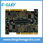
What is a Multilayer PCB?
A Multilayer PCB is a printed circuit board that has more than 2 layers, unlike a double-sided PCB or a 2 layer PCB board, which only has two conductive layers of material. All multilayer PCBs must have at least three layers of conductive material.
A Multilayer PCB is much more complex than a double-sided PCB design and can have any number of conductive copper layers from 4 to 6 layers or even up to 64 layers. Multilayer PCBs are laminated and glued together with layers of heat protection insulation between them. The electrical connections between layers are achieved with various methods such as plating vias, through holes, and buried vias.
What is Gold Finger?
Gold fingers are the gold-plated connectors at the edge of printed circuit boards (PCBs). Shaped like a finger, they serve as connectors that connect the PCB to a motherboard, making sure a signal or command is reliably transmitted.
Before a printed circuit board can be built, it must be designed. This is accomplished using PCB circuit board design CAD tools. PCB design is broken into two main categories: schematic capture to create the circuitry connectivity in a diagram and then PCB layout to design the actual physical circuit board.
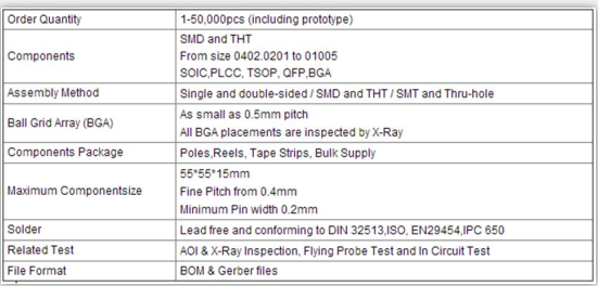
How can we make high quality PCBA products?
Strict incoming material inspection control and management.
Never change BOM indicated material brand without customer’s permission.
Standard Operation Procedure
PCB will be baked in the oven machine in advance.
Fully automatic, high precision SMT and test equipment.
Comprehensive testing include AOI, X-Ray, ICT, software burning according to different PCBAs.
Strict quality management system.
Please send Email to kspcba@c-alley.com or call us through +86 13828766801 Or submit your inquiry by online form. Please fill out below form and attach your manufacturing files( PCB Gerber files and BOM List) if need quotation. We will contact you shortly.
 +86 13828766801
 kspcba@c-alley.com
 https://www.kingshengpcba.com/
 2/F, Building 6, Tangtou 3rd Industrial Zone, Tangtou Community, Shiyan Town, Baoan District, Shenzhen, China, 518108
We would also like to thank our customers for their trust and support. The company's outstanding achievements are mainly due to the loyalty of our customers, which also encourages and spurs our company to forge ahead.
