* On your first PCB Assembly order!
* Up to $300 discount
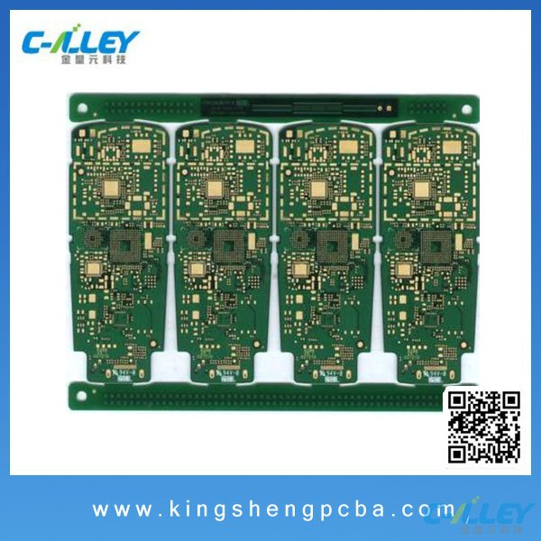
Product Name 0.2 mm BGA Assembly
1.KingshengPCBA Turnkey solution for Meter PCBA/Smart Meter PCBA
2.PCB Assembly, PCB/PCBA Design, PCBA Copy
3.Customized PCBA/OEM/ODM/EMS(Electronics Manufacturing Service)
4.SMT&DIP&PTH&BGA Assembly
5.Component sourcing and purchasing
6.Quick PCBA prototyping
7.Test:X-Ray,AOI,In-Circuit Test(ICT),Functional Test(FCT)
BGA Assembly
The BGA (Ball Grid Array) – Or ball-pin-lattice array package technology is high-density surface assembly packaging technology. At the bottom of the encapsulation, the pins are all spherical and arranged in a lattice-like pattern, thus named BGA. The mainboard control chipset primarily uses this kind of packaging technology, and the material is predominantly ceramic. The memory encapsulated with BGA technology can increase the memory capacity two to three times with the internal volume changes.
BGA minimum size 0.3mm. Our minimum distance to the circuit line is 0.2mm. The minimum length of two BGA is 0.2mm.
Our advanced PCB factory's production capability:
The minimum diameter of the BGA pad is 0.2MM (the sample limit can be 0.15MM).
The minimum BGA to the line is 3MIL (the prototype limit can be 2.5MIL).
The BGA spacing limit is 0.4mm, and the conventional is 0.5mm.
Challenges to the limit are not easy to produce, because the scrap rate is too high, resulting in increased costs.
If you need higher requirements, please make a note.
PCBA Manufacturing Service
PCB files, PCB technical requirements, BOM, Assembly or soldering technical requirements, to be offered by customer.
One Stop PCBA service: Production of PCB from 1-32 Layer, Assembly components/material purchase, SMT production, PCBA Testing, PCBA aging,PCBA Packaging, PCBA Delivery.
PCBA Manufacturing Quality
1. CE-EMC, UL, FCC, SGS, ROHS, ISO9001:2008, ISO14001:2004, TS16949 Certified.
2. 8 Dustproof SMT Lines and DIP Lines.
3. ESD and dust proof working uniform implemented.
4. Operators are strictly trained, and approved for suitable working station.
5. PCBA Production Equipments:HITACHI Screen Printer,FUJI NXT-II & FUJI XPF-L Modules
Automatic Solder-Paste Printer,Reflow Oven,Wave Solder Machine,AI DIP Machine.
6. PCBA Testing Equipments:ORT Machine,Drop Test Machine,Temperature & Humidity Test Chamber, 3D CMM, ROHS Inspection Machine,AOI, X-RAY Inspection.
7. PCBA Testing Capability:AOI(Automatic Optic Inspection),ICT(In-Circuit Test),FCT(Functional Circuit Test),X-Ray for BGAs.
8. Component Package including Component range:
* 01005,0201,0402,0603,0805,1206,1608,2125,3216
* Fine Pitch QFP to 0.2mm
* BGA, Flip Chips, Connectors
* BGA to 0.2mm
9. SOP in every Work Station
10. PCB Materials: FR4, CEM-3, FPC, ALU
PCBA Manufacturing Delivery Duration
Delivery for samples will be 10-15 WD after OEM Contact is signed and the Engineering Documents are confirmed.
For Mass production, based on the customer requirements, delivery can be done in several steps (Partial Delivery).
PCBA Manufacturing Additional Information
1. After the confirmation of Prototype, MP will be started.
2. DIP Components will be positioned only once, minimum distance between components and PCB Board will be maintained.
3. Positioning Holes and Grounding holes will be protected by high temperature resistance tape.
4. EPE Antistatic packaging is used to prevent shock and other problems.
PCBA Shipment
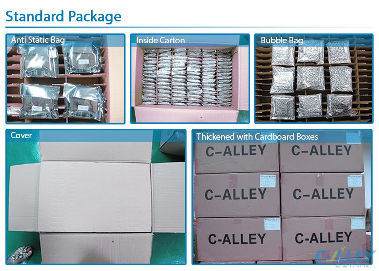
Standard Package
Each PCBA unit will be in Anti static bag, then the bubble bags, and then put into PCBA special carton
Please send Email to kspcba@c-alley.com or call us through +86 13828766801 Or submit your inquiry by online form. Please fill out below form and attach your manufacturing files( PCB Gerber files and BOM List) if need quotation. We will contact you shortly.
 +86 13828766801
 kspcba@c-alley.com
 https://www.kingshengpcba.com/
 2/F, Building 6, Tangtou 3rd Industrial Zone, Tangtou Community, Shiyan Town, Baoan District, Shenzhen, China, 518108
We would also like to thank our customers for their trust and support. The company's outstanding achievements are mainly due to the loyalty of our customers, which also encourages and spurs our company to forge ahead.
